Rapid annealing method for preparing tunneling oxygen passivation contact structure

A contact structure and rapid annealing technology, which is applied in the direction of final product manufacturing, sustainable manufacturing/processing, electrical components, etc., can solve the problems of reducing production efficiency, increasing the surface state density of silicon wafers, and increasing application costs, so as to reduce production Cost, reduction of annealing time, and improvement of production efficiency

Active Publication Date: 2019-08-23
NINGBO INST OF MATERIALS TECH & ENG CHINESE ACADEMY OF SCI
View PDF13 Cites 3 Cited by
  • Summary
  • Abstract
  • Description
  • Claims
  • Application Information

AI Technical Summary

Problems solved by technology

But too high annealing temperature will lead to SiO 2 The thin film responds to the phase transition to produce holes and a large number of dopant atoms in the silicon film diffuse into the silicon matrix
SiO 2 Holes in the film will lead to an increase in the surface state density of the silicon wafer, and a large amount of dopant atom diffusion will increase the Auger recombination in the surface area of ​​the silicon wafer, which will lead to a significant decrease in the passivation performance of the silicon wafer surface
Therefore, in order to ensure the passivation performance, the annealing temperature of the silicon thin film is usually limited to 800-875°C, which leads to a relatively long annealing time.
[0005] Due to the above reasons, the annealing process of the traditional tubular electric furnace usually takes as long as 90-120 minutes, which seriously reduces the production efficiency of this technology and increases the application cost

Method used


Image

  • Rapid annealing method for preparing tunneling oxygen passivation contact structure
  • Rapid annealing method for preparing tunneling oxygen passivation contact structure
  • Rapid annealing method for preparing tunneling oxygen passivation contact structure

Examples


Embodiment 1

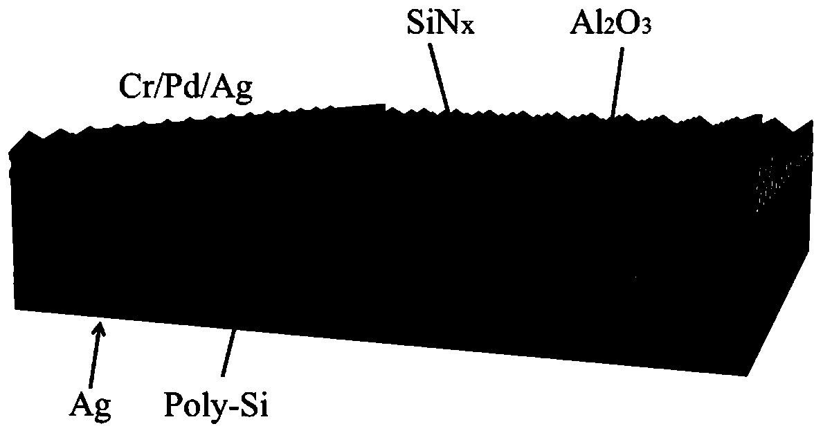
[0036] Double-sided n-TOPCon passivation structure: n + poly-Si / SiO 2 / n c-Si / SiO 2 / n + poly-Si. The basic sample preparation process is as follows: silicon wafer RCA cleaning → hot 68% nitric acid growth ultra-thin oxide layer → PECVD double-sided deposition of phosphorus-doped amorphous silicon 100nm each → rapid annealing.

[0037] The rapid annealing process is:

[0038] (1) Place the sample to be annealed in the equipment, and in a nitrogen atmosphere, first raise the temperature to 200°C at a rate of 15°C / s, and keep it warm for 2 minutes;

[0039] (2) Raise the temperature to 500°C at a rate of 30°C / s and keep warm for 5 minutes;

[0040] (3) Raise the temperature to 800°C at a rate of 10°C / s and keep warm for 5 minutes;

[0041] (3) Cool down to 600°C in 2 minutes, and take out the sample.

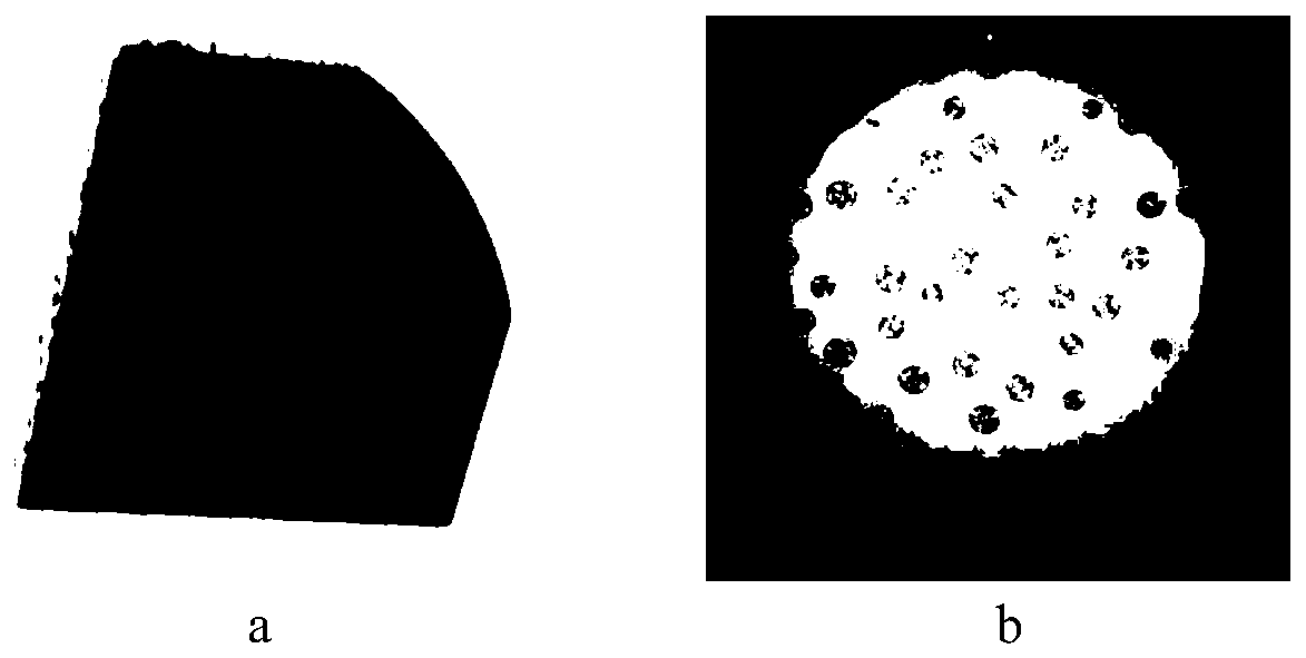
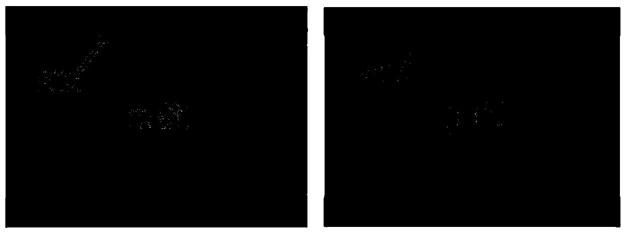
[0042] Using an optical microscope to observe the surface morphology of the polysilicon film, such as Figure 4 As shown, it is confirmed that the membrane structure is co...

Embodiment 2

[0044] Double-sided n-TOPCon passivation structure: n + poly-Si / SiO 2 / n c-Si / SiO 2 / n + poly-Si. The basic sample preparation process is as follows: silicon wafer RCA cleaning → hot 68% nitric acid growth ultra-thin oxide layer → PECVD double-sided deposition of phosphorus-doped amorphous silicon 100nm each → rapid annealing.

[0045] The rapid annealing process is:

[0046] (1) Place the sample to be annealed in the equipment, and in an argon atmosphere, first raise the temperature to 200°C at a rate of 15°C / s, and keep it warm for 2 minutes;

[0047] (2) Raise the temperature to 300°C at a rate of 30°C / s and keep it warm for 1 minute; then raise the temperature to 400°C at a rate of 30°C / s and keep it warm for 1 minute; then raise the temperature to 500°C at a rate of 30°C / s and keep it warm 1 minute; then raise the temperature to 600°C at a rate of 30°C / s, and hold for 1 minute;

[0048] (3) Raise the temperature to 900°C at a rate of 10°C / s and keep it warm for 2 minu...

Embodiment 3

[0052] Double-sided n-TOPCon passivation structure: n + poly-Si / SiO 2 / n c-Si / SiO 2 / n + poly-Si. The basic sample preparation process is as follows: silicon wafer RCA cleaning → hot 68% nitric acid growth ultra-thin oxide layer → PECVD double-sided deposition of phosphorus-doped amorphous silicon 100nm each → rapid annealing.

[0053] The rapid annealing process is:

[0054] (1) Place the sample to be annealed in the equipment, and raise the temperature to 200°C at a rate of 15°C / s in an atmosphere of nitrogen-hydrogen mixture (hydrogen content 5%), and keep it warm for 2 minutes;

[0055] (2) Raise the temperature to 300°C at a rate of 30°C / s and keep it warm for 1 minute; then raise the temperature to 400°C at a rate of 30°C / s and keep it warm for 1 minute; then raise the temperature to 500°C at a rate of 30°C / s and keep it warm 1 minute; then raise the temperature to 600°C at a rate of 30°C / s, and hold for 1 minute;

[0056] (3) Raise the temperature to 700°C at a r...


PUM

PropertyMeasurementUnit
thicknessaaaaaaaaaa
electrical resistivityaaaaaaaaaa
crystallinityaaaaaaaaaa

Abstract

The invention provides a rapid annealing method for preparing a tunneling oxygen passivation contact structure, and the method comprises the following steps: (1) preheating: increasing the temperatureof a sample to be annealed to 150-250 DEG C in process gas, and performing the heat preservation for 1-2min; (2) hydrogen release: increasing the temperature to 300-600 DEG C, and performing heat preservation for 3-10min; (3) crystallization: increasing the temperature to 780-1100 DEG C, and performing heat preservation for 1-15min; (4) cooling: reducing the temperature to 600 DEG C or less within 5 minutes. Through temperature control, the method effectively avoids the phenomenon of film explosion of the sample, and prolongs the body service life of a silicon substrate through hydrogen passivation; meanwhile, doped atoms in a thin film are fully activated; in addition, due to the fact that the annealing time is relatively short, the diffusion degree of doped atoms to the silicon substrate is weakened, the surface auger recombination is effectively reduced, the surface passivation performance of the tunneling oxygen passivation contact structure is improved; meanwhile, the contact resistivity is low; in addition, the annealing time is shortened, the production efficiency is improved, the productivity is improved, and the production cost is saved.

Description

technical field [0001] The invention relates to the technical field of photoelectric material preparation, in particular to an annealing method for a tunneling oxygen passivation contact structure. Background technique [0002] Tunnel Oxygen Passivating Contact (TOPCon, Tunnel Oxide Passivating Contact) structure is composed of high-quality ultra-thin silicon oxide layer (below 2nm) and doped polysilicon film, which can be used as the back surface passivation and carrier of crystalline silicon solar cells transport structure (see figure 1 ). The tunneling oxygen passivation contact structure is characterized by: on the one hand, the ultra-thin silicon oxide layer allows carriers to be transported through the quantum tunneling effect, and at the same time reduces the surface state density of the silicon wafer to achieve chemical passivation; on the other hand, doping The polysilicon and the silicon substrate form a built-in electric field, which not only serves the purpose ...

Claims


Application Information

Patent Timeline
Patent Type & Authority Applications(China)
IPC IPC(8): H01L31/18
CPCH01L31/1864H01L31/1868Y02P70/50
Inventor 廖明墩叶继春曾俞衡闫宝杰杨清张志郭雪琪黄玉清王志学
Owner NINGBO INST OF MATERIALS TECH & ENG CHINESE ACADEMY OF SCI
Why Eureka
Try Eureka