A hydrophobic and quick-drying silicon chip carrier and its preparation method
A carrier and quick-drying technology, which is applied in semiconductor/solid-state device manufacturing, electrical components, nanotechnology, etc., can solve the problems of reducing the surface cleanliness of silicon wafers, affecting the drying effect, increasing drying time, etc., to achieve hydrophobic effect Good, avoid the reduction of acid-base concentration, save time
- Summary
- Abstract
- Description
- Claims
- Application Information
AI Technical Summary
Problems solved by technology
Method used
Image
Examples
Embodiment 1
[0026] 10 Kg of carbon fiber, 5 Kg of carbon black, and 0.5 Kg of graphene are added to 84.5 Kg of polyvinylidene fluoride resin, put into the hopper of a twin-screw extruder, set the heating temperature to 210 degrees, start the twin-screw extruder, and extrude The black round bars are granulated by a granulator for later use.
[0027] After the mold of the injection molding machine undergoes electric discharge treatment, the previous granulation raw materials are used to injection mold to obtain a silicon chip carrier. After testing, the contact angle of the prepared silicon chip carrier is 152°, and the rolling angle is 5.6°. Put the silicon wafer carrier into the water, and after taking it out, the water drops roll off quickly, making it difficult to attach to the silicon wafer carrier, and there is no water mark on the carrier.
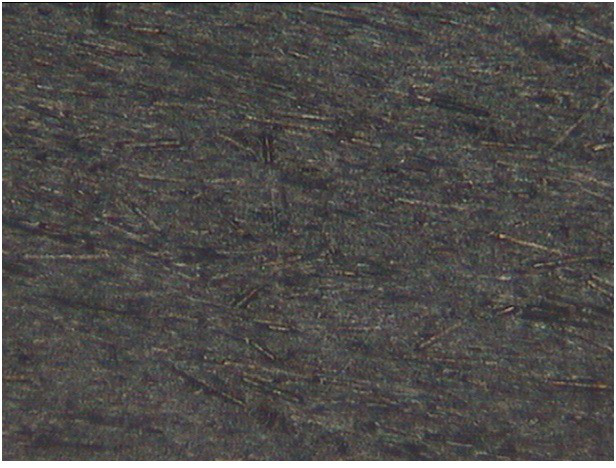
[0028] Figure 1. The surface topography of the injection rod, in which the diameter of the carbon fiber is about 10 microns
Embodiment 2
[0030] 1 Kg of carbon fiber filaments, 10 Kg of carbon black, 0.5 Kg of graphene and 88.5 Kg of polyvinylidene fluoride resin, put into the twin-screw extruder, set the heating temperature to 220 degrees, start the twin-screw extruder, and extrude The black round bars are granulated by a granulator for later use. After the mold of the injection molding machine is corroded by strong acid, the previous granulation raw materials are used, the end plates at both ends of the silicon wafer carrier and the tie rods in the middle are respectively injection molded, and then integrally welded to obtain the silicon wafer carrier. After testing, the contact angle of the prepared silicon wafer carrier was 151°, and the rolling angle was 6.2°. Put the silicon chip carrier into 40% sodium hydroxide aqueous solution, after taking it out, the liquid rolls off quickly, it is difficult to attach to the silicon chip carrier, and there is no liquid residue on the carrier.
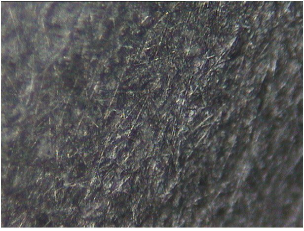
[0031] Figure 2. Topog...
Embodiment 3
[0033]30 Kg chopped carbon fiber, 1 Kg carbon black, 8 Kg graphene and 61 Kg polyvinylidene fluoride resin, add in the twin-screw extruder, set the heating temperature as 220 degrees, start the twin-screw extruder, extruded The black round bars are granulated by a granulator for later use. After the silicon chip carrier rod mold is processed by laser etching, the previous granulation raw materials are used for injection molding to obtain the silicon chip carrier rod. After testing, the contact angle of the tie rod of the prepared silicon wafer carrier was 150°, and the rolling angle was 8.1°. Put the tie bar of the silicon wafer carrier into the 30% sulfuric acid aqueous solution. After taking it out, the liquid rolls off quickly, and it is difficult to attach to the tie rod of the silicon wafer carrier. There is no liquid residue on the railing of the carrier.
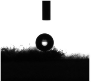
[0034] Figure 3. Topography of the injected tie rod, using carbon fibers with a diameter of 5 μm.
PUM
| Property | Measurement | Unit |
|---|---|---|
| diameter | aaaaa | aaaaa |
| angle | aaaaa | aaaaa |
| angle | aaaaa | aaaaa |
Abstract
Description
Claims
Application Information


