Supercharge Your Innovation With Domain-Expert AI Agents!

Iron oxide photo-anode system with embedded silicon pn junction and fabrication method of iron oxide photo-anode system

An iron oxide light and pn junction technology, applied in photovoltaic power generation, semiconductor devices, final product manufacturing, etc., can solve the problems of small photogenerated voltage, mismatch, carrier recombination, etc., and achieve the effect of ensuring uniformity

Active Publication Date: 2019-09-10
SUZHOU UNIV
View PDF7 Cites 1 Cited by
  • Summary
  • Abstract
  • Description
  • Claims
  • Application Information

AI Technical Summary

Problems solved by technology

[0005] The invention aims to solve the problem that the iron oxide photoanode cannot completely photolyze water in the prior art, and the energy band mismatch of the double-absorbing layer photoelectrode constructed by iron oxide and other light-absorbing layers leads to serious carrier recombination and partial photo-generated voltage. minor technical issues

Method used


Image

  • Iron oxide photo-anode system with embedded silicon pn junction and fabrication method of iron oxide photo-anode system
  • Iron oxide photo-anode system with embedded silicon pn junction and fabrication method of iron oxide photo-anode system
  • Iron oxide photo-anode system with embedded silicon pn junction and fabrication method of iron oxide photo-anode system

Examples


Embodiment 1

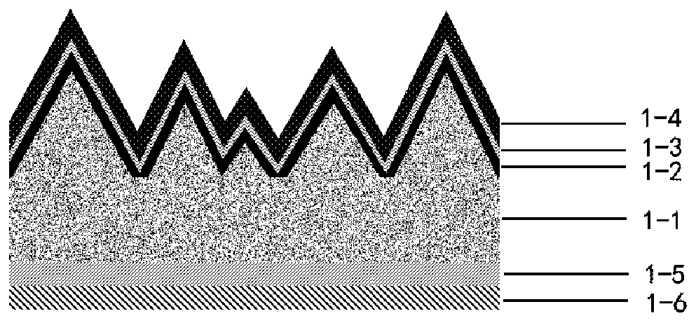
[0037] An iron oxide photoanode system with embedded silicon pn junction, such as figure 1 As shown: the photoanode is a composite layer structure, which sequentially includes an iron oxide absorption layer 1-4, a p-type silicon doped layer 1-2, an n-type silicon substrate 1-1, and a back conductive layer 1 along the light incident direction -5, the back waterproof insulation layer 1-6; the p-type silicon doped layer and the n-type silicon substrate form a silicon pn junction: (1) the morphology of the silicon pn junction is a pyramidal array structure; (2) p-type silicon A transparent conductive tunneling layer 1-3 is disposed between the doped layer 1-2 and the iron oxide absorbing layer 1-4, and the thickness of the transparent conductive tunneling layer is equal everywhere.

[0038] The iron oxide photoanode system with embedded silicon pn junction proposed by the present invention can completely photolyze water. The incident light enters the inside of the photoanode, and...

Embodiment 2

[0040] A method for preparing an iron oxide photoanode system embedded with a silicon pn junction, comprising the following steps:

[0041] 1) Use an n-type silicon wafer with a resistivity of 1-5 Ω·cm to perform standard RCA cleaning.

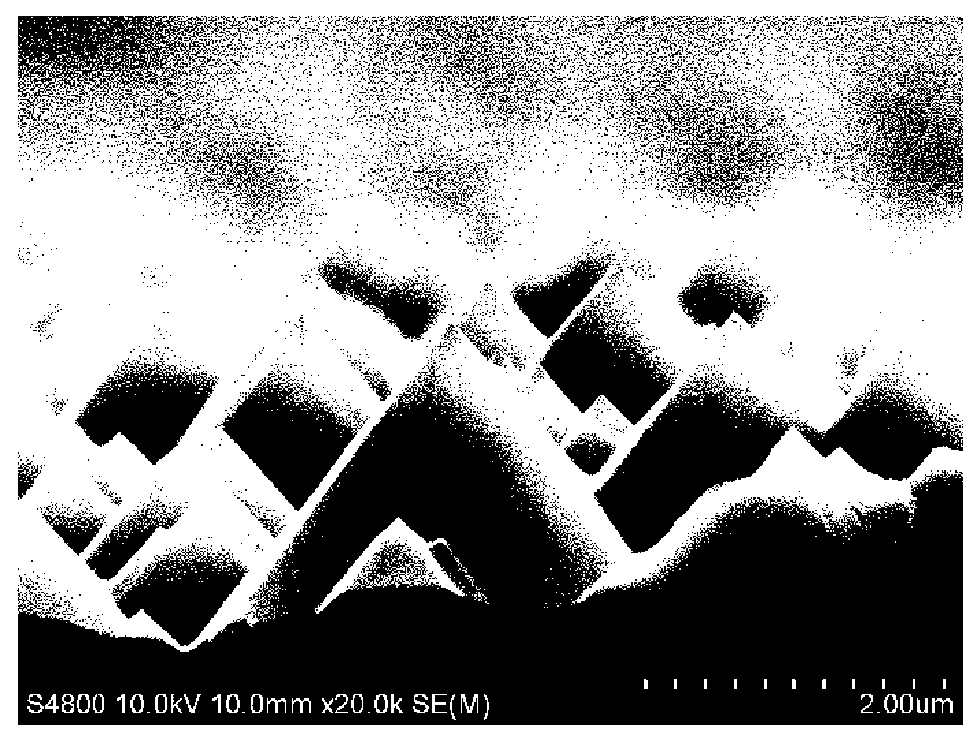
[0042] 2) In a mixed solution of potassium hydroxide and isopropanol, react at 80°C for 60 minutes, and clean the silicon wafer to obtain an n-type silicon pyramid array structure, such as figure 2 shown.

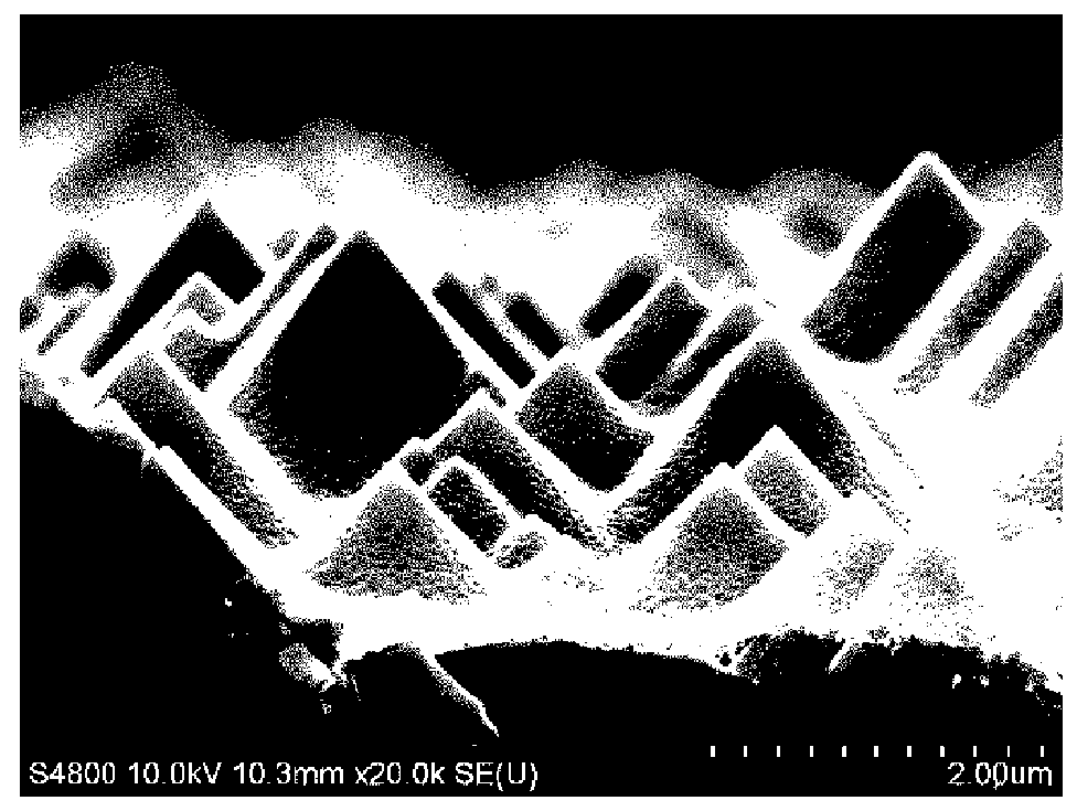
[0043] 3) The n-type silicon pyramid array obtained in step 2) is doped with boron by means of thermal diffusion, and the doping concentration is 2.0×10 19 cm -3 , the junction depth is 200nm. Protect the back side of the n-silicon during thermal diffusion, so that boron doping only occurs on the front side of the silicon pyramid structure.

[0044] 4) Put the prepared silicon pn junction pyramid array into the cavity of the atomic layer deposition system, using tetrakis(dimethylamino)tin as the tin source and tert-butyliminotris(dieth...


PUM

PropertyMeasurementUnit
Thicknessaaaaaaaaaa
Depthaaaaaaaaaa
Thicknessaaaaaaaaaa

Abstract

The invention belongs to the field of photoelectric conversion and new energy. In order to solve the technical problem that complete water photolysis of an iron oxide photo-anode in the prior art cannot be achieved, an iron oxide photo-anode system with an embedded silicon pn junction and a fabrication method of the iron oxide photo-anode system is proposed. The iron oxide photo-anode system comprises an iron oxide absorption layer, a p-type silicon doping layer, an n-type silicon substrate, a back conductive layer and a back waterproof insulation layer, wherein the p-type silicon doping layerand the n-type silicon substrate form a silicon pn junction, the morphology of the silicon pn junction is of a pyramid array structure, and a transparent conductive tunneling layer is arranged between the p-type silicon doping layer and the iron oxide absorption layer. With the embedded silicon pn junction, a relatively large optical voltage is generated when incident light is absorbed by the silicon layer, the optical voltage and the iron oxide can form a series relation, the voltage is equivalently applied to the iron oxide layer, the starting voltage of the iron oxide photo-anode is effectively reduced, the conductivity of the iron oxide absorption layer and the collection efficiency of a photon-generated carrier are improved, so that complete water photolysis is achieved.

Description

technical field [0001] The invention relates to an iron oxide photoanode system and a preparation method embedded with a silicon pn junction, in particular to an energy band interface regulation technology when the photoanode is used for complete photolysis of water, and belongs to the field of photoelectric conversion and new energy. Background technique [0002] The photoelectrochemical cell with the photoelectrode as the core is an effective way to achieve hydrogen production by photolysis of water at low cost with the help of solar energy. It uses the photogenerated carriers generated by semiconductor materials to absorb sunlight to participate in the oxidation and reduction reactions of water (generating hydrogen), that is, to complete the conversion of solar energy into high-energy green fuels. [0003] At present, the application and popularization of hydrogen production by photoelectrochemical cells has encountered many technical difficulties. Among them, the key pr...

Claims


Application Information

Patent Timeline
IPC IPC(8): H01L31/0224H01L31/0352H01L31/04H01L31/18
CPCH01L31/022425H01L31/022466H01L31/035281H01L31/04H01L31/18Y02E10/50Y02P70/50
Inventor 吴绍龙肖臣鸿周忠源李刘晶丁浩李孝峰
Owner SUZHOU UNIV
Features
  • R&D
  • Intellectual Property
  • Life Sciences
  • Materials
  • Tech Scout
  • Unparalleled Data Quality
  • Higher Quality Content
  • 60% Fewer Hallucinations
Learn More