Silicon nitride circuit substrate material and preparation method thereof
A circuit substrate and silicon nitride technology, which is applied in the direction of circuit substrate materials, circuits, printed circuits, etc., can solve the problems of serious surface defects, mechanical properties to be improved, and low pass rate, etc., and achieve a compact structure of the blank and not easy to delaminate Effect of cracking and improving density
- Summary
- Abstract
- Description
- Claims
- Application Information
AI Technical Summary
Problems solved by technology
Method used
Image

Examples
Embodiment 1
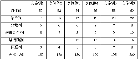
[0028] This embodiment provides a silicon nitride circuit substrate material, which is made of the weight parts of various raw materials as described in Table 1. Wherein, the dispersant is ammonium polyacrylate. The surfactant is cetyltrimethylammonium bromide. The sintering aid is a mixture of silicon magnesium nitride, ytterbium oxide and cerium oxide, and the weight ratio of silicon magnesium nitride: ytterbium oxide: cerium oxide is 3:1:0.8. The coupling agent is 3-aminopropyltriethoxysilane.
[0029] A method for preparing a silicon nitride circuit substrate material, comprising the following steps:
[0030] S1: Mix the coupling agent with 2 / 5 parts by weight of absolute ethanol, stir at room temperature at a speed of 200r / min for 10 minutes, add carbon fibers to soak for 30 minutes, add the remaining 3 / 5 parts by weight of absolute ethanol, nitrogen Silica, dispersant, surfactant, sintering aid, keep the speed constant, continue to stir for 1.5h, to obtain the mixture...
Embodiment 2
[0035] This embodiment provides a silicon nitride circuit substrate material, which is made of the weight parts of various raw materials as described in Table 1. Wherein, the dispersant is calcium lignosulfonate. The surfactant is sodium dodecylbenzenesulfonate. The sintering aid is a mixture of silicon magnesium nitride, ytterbium oxide and cerium oxide, and the weight ratio of silicon magnesium nitride: ytterbium oxide: cerium oxide is 3: 2: 1.5. The coupling agent is vinyltrichlorosilane.
[0036] A method for preparing a silicon nitride circuit substrate material, comprising the following steps:
[0037] S1: Mix the coupling agent with 2 / 5 parts by weight of absolute ethanol, stir at room temperature at a speed of 200r / min for 10 minutes, add carbon fibers to soak for 30 minutes, add the remaining 3 / 5 parts by weight of absolute ethanol, nitrogen Silica, dispersant, surfactant, sintering aid, keep the speed constant, continue to stir for 2h, to obtain the mixture;
[0...
Embodiment 3
[0042] This embodiment provides a silicon nitride circuit substrate material, which is made of the weight parts of various raw materials as described in Table 1. Wherein, the dispersant is ammonium polyacrylate. The surfactant is sodium dodecylbenzenesulfonate. The sintering aid is a mixture of silicon magnesium nitride, ytterbium oxide and cerium oxide, and the weight ratio of silicon magnesium nitride: ytterbium oxide: cerium oxide is 3:1.5:1. The coupling agent is 3-aminopropyltriethoxysilane.
[0043] A method for preparing a silicon nitride circuit substrate material, comprising the following steps:
[0044] S1: Mix the coupling agent with 2 / 5 parts by weight of absolute ethanol, stir at room temperature at a speed of 200r / min for 10 minutes, add carbon fibers to soak for 30 minutes, add the remaining 3 / 5 parts by weight of absolute ethanol, nitrogen Silica, dispersant, surfactant, sintering aid, keep the speed constant, continue to stir for 2h, to obtain the mixture; ...
PUM
| Property | Measurement | Unit |
|---|---|---|
| length | aaaaa | aaaaa |
| bending strength | aaaaa | aaaaa |
| particle size | aaaaa | aaaaa |
Abstract
Description
Claims
Application Information
 - R&D
- Intellectual Property
- Life Sciences
- Materials
- Tech Scout
- Unparalleled Data Quality
- Higher Quality Content
- 60% Fewer Hallucinations
Browse by: Latest US Patents, China's latest patents, Technical Efficacy Thesaurus, Application Domain, Technology Topic, Popular Technical Reports.
© 2025 PatSnap. All rights reserved.Legal|Privacy policy|Modern Slavery Act Transparency Statement|Sitemap|About US| Contact US: help@patsnap.com