Low-power-consumption nerve synapse thin film transistor and preparation method thereof

A technology of thin film transistors and neural synapses, which is applied in the direction of transistors, semiconductor/solid-state device manufacturing, semiconductor devices, etc., can solve the problems of difficult large-scale integration of organic materials, inability to update weights, difficult large-scale integration, etc., to meet the requirements of Flexible and biocompatible, improve functionality and practicality, and achieve the effect of remembering time

Active Publication Date: 2019-11-05
FUDAN UNIV
View PDF4 Cites 12 Cited by
  • Summary
  • Abstract
  • Description
  • Claims
  • Application Information

AI Technical Summary

Problems solved by technology

[0003] The resistive variable memory at both ends can simulate typical synaptic behavior, but the weight update cannot be performed in the case of canceling the signal transmission between neurons, and it is difficult to have very low power consumption due to the mechanism of its ion movement leading to synaptic behavior; Synapse transistors with organic nanowire structures can achieve power

Method used


Image

  • Low-power-consumption nerve synapse thin film transistor and preparation method thereof
  • Low-power-consumption nerve synapse thin film transistor and preparation method thereof
  • Low-power-consumption nerve synapse thin film transistor and preparation method thereof

Examples


preparation example Construction

[0040] A method for preparing a low-power synapse thin film transistor, including:

[0041] (1) A gate dielectric layer with a thickness of 20-150nm is grown on the upper surface of the back gate electrode by atomic deposition technology. During the preparation process, the temperature is controlled at 30-150°C, and the power of oxygen plasma is 1500-2500 W. The flow rate is 100-180sccm;

[0042] (2) Using physical vapor deposition technology to grow and etch the upper surface of the gate dielectric layer to obtain a conductive channel with a thickness of 30-80nm. During the preparation process, the chamber pressure of the magnetron sputtering is controlled to be 0.5-2Pa, and the temperature is room temperature. The length and width of the channel formed on the upper surface of the source-drain electrode are 5-10 μm and 50-150 μm, respectively;

[0043] (3) Prepare source-drain electrodes by electron beam evaporation;

[0044] (4) performing thermal annealing in a nitrogen a...

Embodiment 1

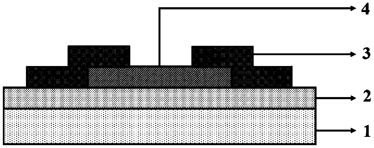
[0047] An all-inorganic low-power synapse thin film transistor provided in this embodiment has a structure such as figure 1 As shown, the transistor structure from bottom to top is: back gate electrode 1, gate dielectric layer 2, conductive channel 3 and source-drain electrode 4. The source-drain electrode 4 is arranged on the upper surface of the gate dielectric layer 2 , the conductive channel 3 is located on the upper surface and both sides of the source-drain electrode 4 , and a channel is formed on the upper surface of the source-drain electrode 4 .

[0048] The specific preparation process of the transistor is as follows:

[0049] (1) A low-resistance heavily doped p-type silicon substrate is selected for the back gate electrode 1, and the resistivity is <0.005Ω·cm.

[0050] (2) The gate dielectric layer 2 is made of aluminum oxide, using trimethylaluminum (TMA) and oxygen plasma as the precursor and reactant respectively, and grown on the back gate electrode 1 by atomi...

Embodiment 2

[0057] A low-power neural synapse thin film transistor, from bottom to top: a back gate electrode, a gate dielectric layer, a conductive channel, and a source-drain electrode, the source-drain electrode is arranged on the upper surface of the gate dielectric layer, and the conductive channel It is located on the upper surface and both sides of the source-drain electrode, and a channel is formed on the upper surface of the source-drain electrode.

[0058] In this embodiment, the gate dielectric layer is HfO 2 、TiO 2 Composite material, the conductive channel is SnO 2 , the back gate electrode is a low-resistance silicon substrate with a resistivity <0.005Ω·cm. The material selected for the source-drain electrodes is Ti / Au. The synaptic behavior is realized through electron trapping and release through the defects at the interface between the gate dielectric layer and the conductive channel. The defects at the interface between the gate dielectric layer and the conductive ch...


PUM

PropertyMeasurementUnit
Thicknessaaaaaaaaaa
Widthaaaaaaaaaa

Abstract

The invention relates to a low-power-consumption neural synapse thin film transistor and a preparation method thereof. The transistor structurally comprises a back gate electrode, a gate dielectric layer, a conductive channel and a source-source electrode from bottom to top in sequence. The source-drain electrode is arranged on the upper surface of the gate dielectric layer, and the conductive channels are located on the upper surface and two sides of the source-drain electrode; channels are formed on the upper surface of the source-drain electrode. Compared with the prior art, the transistorhas ultra-low power consumption at a normal focus level; the adjustable memory time from milliseconds to thousands of seconds can be realized at different dielectric layer preparation temperatures; meanwhile, the stability of the transistor is greatly improved due to the use of a full-inorganic material; the flexibility and synaptic performance of the transistor can be used for flexible electronics and large-scale neuromorphic circuit systems.

Description

technical field [0001] The invention belongs to the field of semiconductor devices, in particular to a low-power synapse thin film transistor and a preparation method thereof. Background technique [0002] Our brain is a brain with ~10 11 neurons and ~10 15 A complex network with highly interconnected synapses, massive parallelism, and variable structure. Inspired by the human brain, large-scale neuromorphic circuit systems with distributed information storage and parallel architecture information processing are much more efficient and adaptable in complex environments than traditional von Neumann computing systems based on centralized sequential operations many. Synapses are the fundamental units that connect neurons and establish neuromorphic structures in biological systems. Therefore, synaptic devices capable of simulating the behavior of biological synapses are essential for constructing neuromorphic electronic systems. But the key to neurosynaptic devices is not o...

Claims


Application Information

Patent Timeline
IPC IPC(8): H01L29/786H01L29/51H01L21/34
CPCH01L29/517H01L29/66969H01L29/7869H01L29/78693
Inventor 丁士进李凌凯邵龑吴小晗
Owner FUDAN UNIV
Why Eureka
Try Eureka