Preparation method of vanadium oxide film

A vanadium oxide thin film and seed layer technology, which is applied in gaseous chemical plating, vacuum evaporation plating, coating, etc., can solve the problem of poor uniformity of vanadium oxide thin film sheet resistance, unfavorable product quality consistency, and poor film uniformity, etc. problems, to achieve high practical value, suitable for large-scale production, and good uniformity

Active Publication Date: 2019-11-15
INST OF MICROELECTRONICS CHINESE ACAD OF SCI
View PDF7 Cites 0 Cited by
  • Summary
  • Abstract
  • Description
  • Claims
  • Application Information

AI Technical Summary

Problems solved by technology

[0004] A single vanadium oxide film is used as thermistor material, mainly VO 2 film, due to VO 2 The sheet resistance of the thin film is easily affected by various factors such as substrate temperature, crystallization degree, vanadium oxide crystal orientation distribution, valence distribution and other factors during the preparation process, resulting in poor uniformity of internal resistance of the prepared vanadium oxide thin film, which is not conducive to Product Quality Consistency
In addition, for the thicker vanadium oxide film, during the deposition process, with the prolongation of the deposition time, the film resistivity will be significantly smaller, and the film uniformity will also be poor, which exceeds the product's requirements for resistance and will also cause Decrease in TCR

Method used


Image

  • Preparation method of vanadium oxide film
  • Preparation method of vanadium oxide film
  • Preparation method of vanadium oxide film

Examples


Embodiment 1

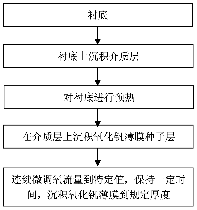
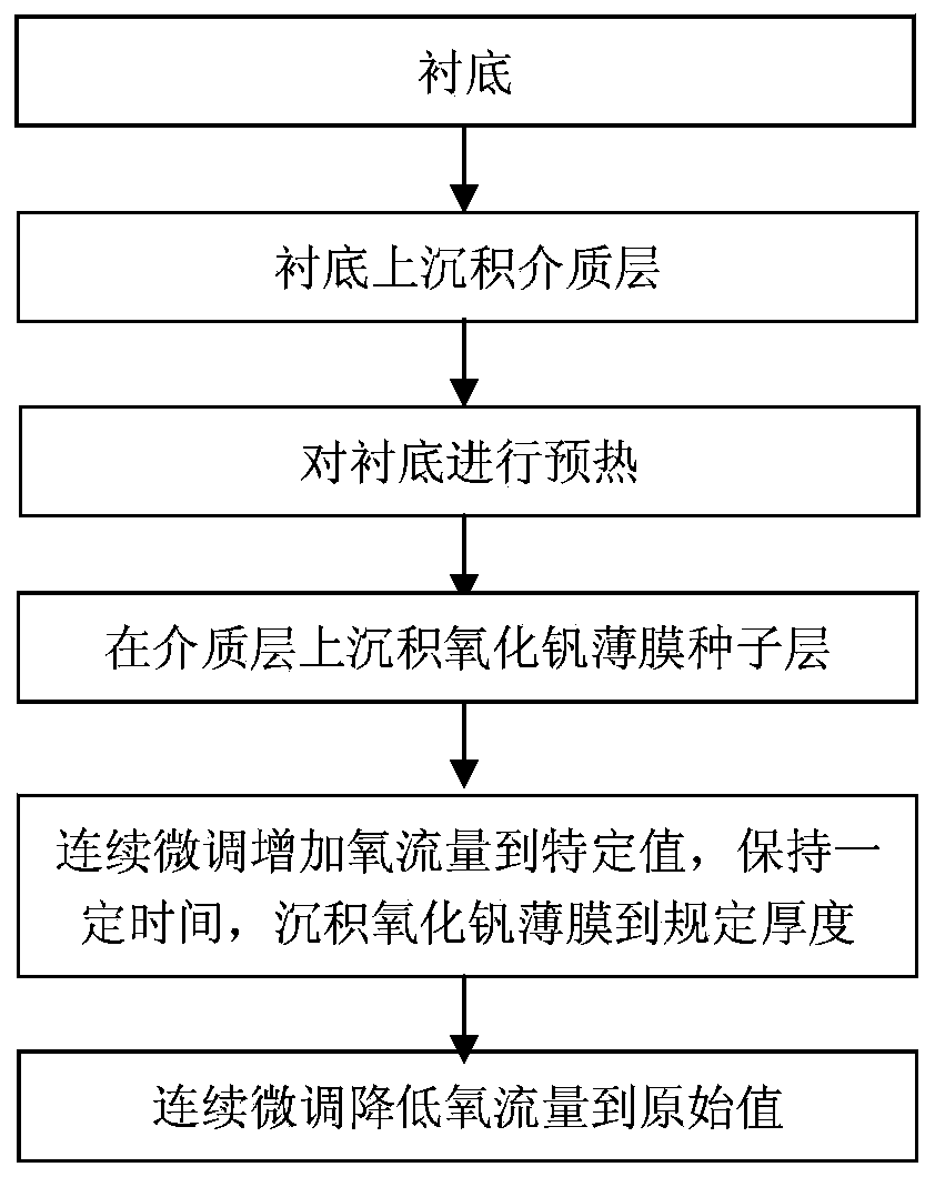
[0030] figure 1 A flowchart of manufacturing a microelectrode structure according to an embodiment of the disclosure is shown.

[0031] In this embodiment, the preparation method of the vanadium oxide film includes:

[0032] S101. Provide a substrate. In this embodiment, the substrate can be in various forms, including but not limited to semiconductor material substrates (such as bulk Si substrates), compound semiconductor substrates (such as SiC substrates), alloy semiconductor substrates (such as SiGe substrate) and so on. In some embodiments, the semiconductor substrate may include a doped epitaxial layer.

[0033] S102, forming a dielectric layer above the substrate. A dielectric layer is deposited on the above substrate. In some embodiments, the dielectric layer includes any one or a combination of insulating materials selected from silicon nitride, silicon dioxide, and silicon carbide, and mainly functions as an insulating layer. In some embodiments, any one of various depo...

Embodiment 2

[0038] S101. Provide a substrate. In this embodiment, the substrate may be a substrate of various forms. In this embodiment, the preferred substrate is a Si substrate.

[0039] S102, forming a dielectric layer above the substrate. A dielectric layer is deposited on the above-mentioned substrate. In this embodiment, the dielectric layer is preferably silicon nitride as the dielectric layer (ie, insulating layer), which mainly plays a role of insulation. In this embodiment, the dielectric layer is mainly formed by chemical vapor deposition technology; the specific process conditions of chemical vapor deposition are as follows: deposition temperature 250°C, RF power 400W, SiH4: 300 sccm, N2: 4000 sccm, NH3: 100 sccm, pressure: 5 Torr_ .

[0040] S103: Preheat the substrate. The preheating temperature for preheating the substrate is preferably 200°C, and the preheating time is preferably 5 minutes.

[0041] S104. Using magnetron sputtering to form a vanadium oxide thin film seed laye...

Embodiment 3

[0044] S101. Provide a substrate. In this embodiment, the substrate may be a substrate of various forms. In this embodiment, the substrate is preferably a silicon substrate.

[0045] S102, forming a dielectric layer above the substrate. A dielectric layer is deposited on the above-mentioned substrate. In this embodiment, the dielectric layer is preferably silicon dioxide as the dielectric layer (ie, insulating layer), which mainly plays a role of insulation. In this embodiment, the dielectric layer is mainly formed by chemical vapor deposition technology; the specific process conditions of chemical vapor deposition are as follows: deposition temperature 250° C., RF power 400 W, SiH4: 35 sccm, N2O: 1200 sccm, and pressure: 2.7 Torr_.

[0046] S103: Preheat the substrate. The preheating temperature for preheating the substrate is preferably 150°C, and the preheating time is preferably 5 minutes.

[0047] S104. Using magnetron sputtering to form a vanadium oxide thin film seed layer ...


PUM

PropertyMeasurementUnit
thicknessaaaaaaaaaa
thicknessaaaaaaaaaa
thicknessaaaaaaaaaa

Abstract

The invention provides a preparation method of a vanadium oxide film. The preparation method of the vanadium oxide film is characterized by comprising the following steps: providing a substrate; depositing a dielectric layer above the substrate; preheating the substrate; forming a vanadium oxide film seed layer on the dielectric layer by a magnetron sputtering method, wherein the process conditions of forming the vanadium oxide film seed layer are as follows: radio frequency sputtering power is 500 to 1000 W, oxygen flow is 6 to 10 sccm, argon flow is 50 sccm, working pressure is 0.1 to 3 Pa and the temperature of the substrate is 150 to 250 DEG C; and gradually and continuously performing fine adjustment on the oxygen flow to a predetermined value while maintaining other process conditions of magnetron sputtering not to be changed, depositing a vanadium oxide film on the vanadium oxide film seed layer until the specified thickness, wherein continuous fine adjustment of oxygen flow isstepped as 0.1 to 1 sccm, the duration time at each step is 1 to 30 seconds, a certain time is maintained after the fine adjustment oxygen reaches to the predetermined value and the vanadium oxide film is deposited to the specified thickness. By the method provided by the invention, the vanadium oxide film obtained through deposition has the advantages of single and uniform film tissue structureand the like; furthermore, the preparation method is simple and easy to operation, is suitable for large-scale production and has high practical value.

Description

Technical field [0001] The invention relates to the technical field of uncooled infrared detection, in particular to a method for preparing a vanadium oxide film. Background technique [0002] Infrared detectors convert invisible infrared heat radiation into detectable electrical signals, enabling observation of external affairs. Infrared detectors are divided into quantum detectors and thermal detectors. Heat detectors are also called uncooled infrared detectors. Uncooled infrared detectors have low cost, no need for cooling, can work at room temperature, and have the advantages of good stability, high integration, and low price. They are used in military, commercial and civilian applications. There are broad application prospects in such fields. Uncooled infrared detectors mainly include pyroelectrics, thermocouples, and thermistors. Among them, the focal plane detector of the microbolometer based on the thermistor, the principle is that when the external infrared radiation e...

Claims


Application Information

Patent Timeline
Patent Type & Authority Applications(China)
IPC IPC(8): C23C14/08C23C14/35C23C16/40
CPCC23C14/083C23C14/35C23C16/402
Inventor 高建峰李俊峰刘卫兵赵超王文武
Owner INST OF MICROELECTRONICS CHINESE ACAD OF SCI
Why Eureka
Try Eureka