Wafer level packaging MEMS chip structure and processing method thereof

A wafer-level packaging and chip structure technology, used in microstructure technology, microstructure devices, manufacturing microstructure devices, etc., can solve the problems of poor sealing and large drift of characteristic parameters, achieve good packaging sealing and reduce wiring difficulty. , the effect of avoiding air leakage

Active Publication Date: 2019-11-19
BEIJING INST OF AEROSPACE CONTROL DEVICES
View PDF7 Cites 19 Cited by
  • Summary
  • Abstract
  • Description
  • Claims
  • Application Information

AI Technical Summary

Problems solved by technology

[0006] In order to overcome the problems of poor vacuum package sealing and large drift of characteristic parameters under different temperature conditions in the existing wafer-level packaging MEMS chips based on TSV technology, the present invention proposes A wafer-level packaging MEMS chip structure and its processing method are proposed, which combine lateral electrode extraction and vertical TSV vertical electrode extraction

Method used


Image

  • Wafer level packaging MEMS chip structure and processing method thereof
  • Wafer level packaging MEMS chip structure and processing method thereof
  • Wafer level packaging MEMS chip structure and processing method thereof

Examples


Embodiment 1

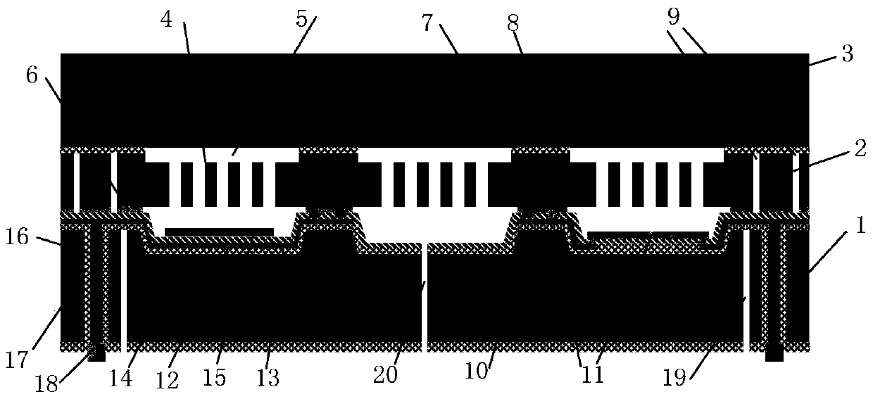
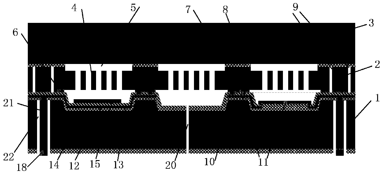
[0083] The cavity depth of the substrate sheet of the present invention is 2 μm-20 μm, the thickness of the first silicon oxide layer 14 is 1 μm-3 μm; the first metal electrode layer 15 is made of tungsten, aluminum, titanium, copper, gold, nickel, chromium, tantalum, cobalt One or more compositions, the thickness is 100nm-300nm; the thickness of the second silicon oxide layer 16 is 300nm-600nm, and the second metal layer 11 is also used as a bonding medium layer including an adhesion barrier layer and a metal eutectic solder layer , the adhesion barrier layer adopts one or several combinations of Cr, Ti, Ni, W, and the metal eutectic solder layer adopts one of AuSi, AuSn, AlGe, CuSn; the thickness of the adhesion barrier layer is 10nm-50nm; the metal eutectic solder layer The thickness of the crystal solder layer is 0.5 μm-2 μm; in the cavity on the substrate layer, there is also a getter layer 18; the getter is Ti, Zr, V or a combination of several kinds. The thickness of th...

Embodiment 2

[0088] The first process is the processing of the device layer and the capping layer. The processing flow is shown in Figure 2. The detailed processing process is described as follows in conjunction with Figure 2:

[0089] 1) Silicon oxidation of the device layer, such as Figure 2a ;

[0090] 2) Etch silicon oxide by photolithography, and form a silicon oxide pattern consistent with the pattern of the anchor region on the bonding surface, such as Figure 2b ;

[0091] 3) The silicon wafer of the device layer is subjected to photolithography and dry etching to form an anchor region pattern, such as Figure 2c shown;

[0092] 4) The device layer silicon wafer and the cap layer silicon wafer are directly bonded to silicon-silicon oxide, such as Figure 2d shown;

[0093] 5) Thinning the device layer silicon wafer, such as Figure 2e shown;

[0094]6) The device layer is subjected to photolithography and dry etching to realize the etching of the microstructure on the devic...


PUM

PropertyMeasurementUnit
thicknessaaaaaaaaaa
depthaaaaaaaaaa
thicknessaaaaaaaaaa

Abstract

The invention relates to a wafer level packaging MEMS chip structure and a processing method thereof, and the structure forms a cavity structure for the movement of a comb tooth microstructure of a device layer through the sequential bonding of a cap layer, the device layer and a substrate layer. Electrical signals in the packaging cavity are led out from the side surface of the structure by crossing a substrate bonding sealing ring by a first-layer lead of a double-layer metal lead arranged on the substrate layer; after metal eutectic bonding wafer-level vacuum packaging is completed, deep silicon etching is carried out at a position corresponding to a metal electrode on the back surface of a substrate wafer to form a through hole, a conductive material is used for filling the through hole or forming a conductive silicon column, and electrode leading-out is carried out on the back surface. The structure can be integrated with a signal processing circuit in a flip-chip bonding mode. Compared with a mode of manufacturing a TSV through hole in a packaging cavity for electrical lead-out, the problem of packaging air tightness caused by filling a cavity with an insulating medium is avoided, and the problems of temperature stability and reliability caused by mismatching of thermal expansion coefficients of a filling material and a silicon material are also avoided.

Description

technical field [0001] The invention belongs to the technical field of micro-electromechanical systems (MEMS) manufacturing, and in particular relates to a wafer-level packaging MEMS chip structure and a processing method thereof. Background technique [0002] Wafer-level packaging technology, through wafer bonding, realizes airtight or vacuum packaging of devices on the entire wafer at one time, and completes the mechanical and electrical connections between different structural levels of MEMS chips. The packaging process is simplified, the packaging cost is reduced, and the overall outline size of the device is also greatly reduced. Wafer-level vacuum packaging can maximize the protection of movable structures in MEMS devices from water flow and particle pollution during the scribing process, which is conducive to reducing batch costs and improving product consistency, yield and reliability. [0003] The longitudinal vertical electrode lead-out technology is adopted to re...

Claims


Application Information

Patent Timeline
Patent Type & Authority Applications(China)
IPC IPC(8): B81B7/00B81C1/00
CPCB81B7/0032B81B7/0006B81C1/00261
Inventor 张乐民刘福民穆京京刘宇张树伟杨静刘国文梁德春吴浩越崔尉
Owner BEIJING INST OF AEROSPACE CONTROL DEVICES
Why Eureka
Try Eureka