Regrowth method for reducing interface state of HEMT device by utilizing InN protection layer and HEMT device
A protective layer and interface state technology, which is applied in semiconductor devices, semiconductor/solid-state device manufacturing, electrical components, etc., can solve the problems of difficult control of etching depth, lower device reliability, and surface leakage, so as to avoid high source and drain Effects of contact resistance, interface damage, reliability improvement, and interface quality improvement
- Summary
- Abstract
- Description
- Claims
- Application Information
AI Technical Summary
Problems solved by technology
Method used
Image
Examples
Embodiment 1
[0034] A kind of regrowth method that utilizes InN protection layer to reduce interface state of HEMT device, its step comprises:
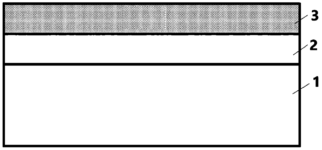
[0035] (1) if figure 1 As shown, after the GaN layer 1 and the AlGaN layer 2 are grown in the MOCVD system, a 10-20nm InN protective layer 3 is grown in situ. The growth temperature of InN is about 500°C, the growth time is about 5-9min, and the gas source is trimethylindium and ammonia;
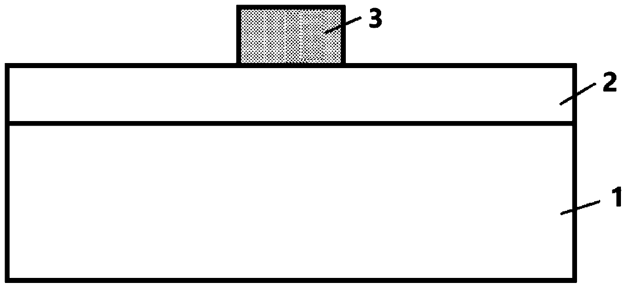
[0036] (2) Spin-coat a layer of photoresist on the InN protective layer, transfer the pattern on the photoresist, and then use the photoresist as a mask to remove the InN protective layer 3 other than the gate to obtain the following: figure 2 the structure shown;
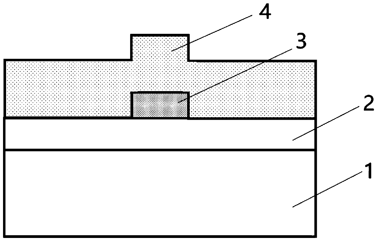
[0037] (3) Deposit a mask layer 4 on the surface of the AlGaN / GaN substrate by PECVD, such as image 3 As shown, the mask layer is then patterned by photolithography and RIE fluorine-based ion etching to obtain the Figure 4 the structure shown;
[0038] (4) Put the substrate with the mask patt...
Embodiment 2
[0042] A kind of regrowth method that utilizes InN protection layer to reduce interface state of HEMT device, its step comprises:
[0043] (1) if Figure 10 As shown, after the GaN layer 1 and the AlGaN layer 2 are grown in the MOCVD system, a GaN layer 9 with a thickness of 2-4 nm is grown in situ on the AlGaN layer, and then a 10-20 nm InN protective layer 3 is grown in situ. The growth temperature is about 500°C, the growth time is about 5-9min, and the gas source is trimethylindium and ammonia;
[0044] (2) Spin-coat a layer of photoresist on the InN protective layer, transfer the pattern on the photoresist, and then use the photoresist as a mask to remove the InN protective layer 3 other than the gate;
[0045] (3) Deposit a mask layer on the surface of the AlGaN / GaN substrate by PECVD, and pattern the mask layer by photolithography and RIE fluorine-based ion etching;
[0046](4) Put the substrate with the mask pattern into the MOCVD system to heat up to decompose the I...
PUM
| Property | Measurement | Unit |
|---|---|---|
| Thickness | aaaaa | aaaaa |
| Thickness | aaaaa | aaaaa |
Abstract
Description
Claims
Application Information


