Novel die bonding film

A die-bonding and thin-film technology, which is applied in the fields of interconnection and third-generation semiconductor packaging die-bonding, can solve the problems of high surface energy, easy oxidation and vulcanization, etc., and achieve the effect of high Young's modulus

Active Publication Date: 2020-01-07
SOUTH UNIVERSITY OF SCIENCE AND TECHNOLOGY OF CHINA
View PDF10 Cites 1 Cited by
  • Summary
  • Abstract
  • Description
  • Claims
  • Application Information

AI Technical Summary

Problems solved by technology

Although this method also takes advantage of the small size of nano-metals to achieve low-temperature interconnection, many nano-metal powders are very prone to oxidation and vulcanization due to high surface energy because no other protection is added.
Therefore, this method also has some limitations

Method used


Image

  • Novel die bonding film
  • Novel die bonding film

Examples


Embodiment 1

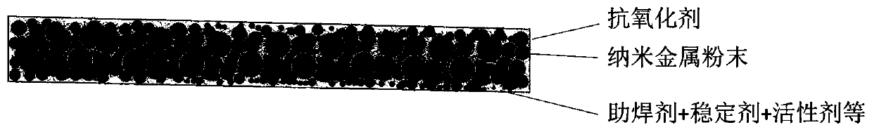
[0024] This embodiment proposes a new type of crystal-bonding film, such as figure 1 As shown, it is a schematic diagram of a new type of crystal-bonding film, which is characterized in that it includes nano-metal powder, antioxidant, flux, stabilizer, and active agent, wherein the nano-metal powder is metal Au as the shell layer, and Cu is the core-shell structure of the core layer , the metal powder content is 65wt.%, the antioxidant polyethylene glycol and oleic acid mixture content is 30wt.%, the flux-activating rosin content is 1wt.%, the stabilizer is polyvinylpyrrolidone (PVP), and the active agent is mainly composed of Zinc chloride, wherein the total amount of flux, stabilizer and active agent is ≤10.0wt.%. The role of the active agent is to remove oxides on the surface of the nano-metal, reduce the surface tension of the molten nano-metal material, improve its wettability, and prevent secondary oxidation during the sintering process. Such as figure 2 Shown is a sc...

Embodiment 2

[0028] This embodiment proposes a new type of crystal-bonding film, such as figure 1 As shown, it is a schematic diagram of a new type of crystal-bonding film, which is characterized in that it includes nano-metal powder, antioxidant, flux, stabilizer, and active agent, wherein the nano-metal powder is Cu powder, and the content of Cu powder is 50wt.%. Antioxidant three Ethanolamine, the content is 40wt.%, the flux stearic acid content is 3wt.%, the stabilizer is cetyl ammonium bromide (CTAB), and the main component of the active agent is citric acid, wherein the flux, stabilizer and active agent Total amount≤10.0wt.%. The role of the active agent is to remove oxides on the surface of the nano-metal, reduce the surface tension of the molten nano-metal material, improve its wettability, and prevent secondary oxidation during the sintering process. Nano-Cu powder, antioxidant, soldering flux, stabilizer, and activator are mixed and pressed to form a dark film with a thickness o...


PUM

PropertyMeasurementUnit
thicknessaaaaaaaaaa
thicknessaaaaaaaaaa
thicknessaaaaaaaaaa

Abstract

The invention discloses a novel die bonding film. The film is characterized by comprising nano metal powder, antioxidant, soldering flux, stabilizer and active agent, wherein the content of the nano metal powder is 40-95.0 wt.%, the content of the antioxidant is 1-50 wt.%, the content of the soldering flux is 1-50.0 wt.%, and the total amount of the soldering flux, the stabilizer and the active agent is smaller than or equal to 10.0 wt.%. The film is advantaged in that the nanometer metal powder, the antioxidant, the soldering flux and other materials are mixed and pressed to form a film, highheat dissipation can be achieved, thickness is uniform, flatness of a die bonding layer is well controlled, die bonding and interconnection under the low-temperature condition are achieved on the premise that electrical performance of a semiconductor packaging interconnection module is not affected, and use under the conditions of small spacing, high power, high temperature, high pressure and thelike can be met. The solid crystal film can be used in the fields of power electronic application, IGBT packaging, photoelectron packaging, MEMS packaging, microelectronics, high-power LED packagingand the like.

Description

technical field [0001] The invention belongs to the field of third-generation semiconductor packaging crystal bonding and interconnection, and in particular relates to a novel crystal bonding film. Background technique [0002] Electronic interconnection materials are the hub of semiconductor device manufacturing, microelectronic packaging, and power electronic packaging microdevice module connection components. As a representative die-bonding and interconnection material in the modern electronics industry, tin brazing materials are widely used. However, with the rapid development of third-generation semiconductor materials and their components, microelectronic systems are developing in the direction of high power, high-density integration, miniaturization, and multi-functionalization. Management and other aspects put forward higher requirements, such as realizing high-temperature resistant interconnection (greater than 200°C) or multi-level packaging requires pre-level inte...

Claims


Application Information

Patent Timeline
Patent Type & Authority Applications(China)
IPC IPC(8): H01L23/488B82Y30/00
CPCB82Y30/00H01L24/29H01L2224/29139H01L2224/29147H01L2224/2957H01L2224/2969
Inventor 崔成强杨斌叶怀宇张国旗
Owner SOUTH UNIVERSITY OF SCIENCE AND TECHNOLOGY OF CHINA
Why Eureka
Try Eureka