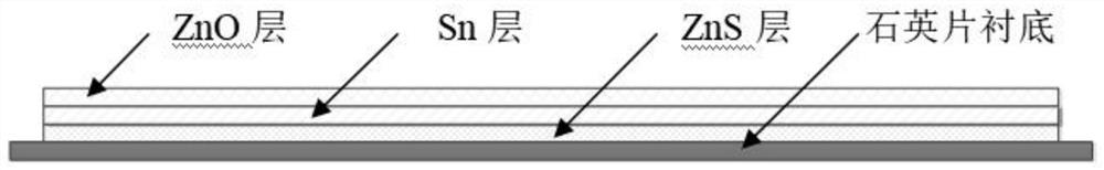
A kind of zns/sn/zno heterostructure film material and its preparation method and application
A thin film material and heterostructure technology, applied in metal material coating process, vacuum evaporation coating, coating and other directions, can solve the problems of slow response speed, wide band gap, weak light absorption, etc., to achieve fast response speed, The effect of narrow band gap and small lattice mismatch
- Summary
- Abstract
- Description
- Claims
- Application Information
AI Technical Summary
Problems solved by technology
Method used
Image

Examples
preparation example Construction
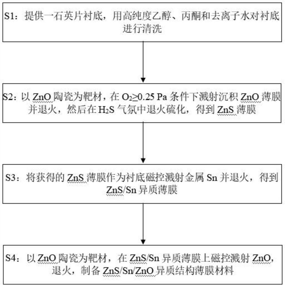
[0035] The present invention provides a preparation method of the ZnS / Sn / ZnO heterostructure thin film material described in the above technical solution, comprising the following steps:
[0036] Using ZnO ceramics as the target material, the first sputtering is carried out on the substrate to obtain ZnO thin film;
[0037] performing a first annealing treatment on the ZnO film in an air atmosphere, and performing sulfuration annealing on the obtained film in a sulfide gas to obtain a ZnS film;
[0038] Using the ZnS thin film as a substrate, and using single crystal Sn as a target, sequentially performing a second sputtering and a second annealing treatment to obtain a ZnS / Sn thin film;
[0039] Using the ZnS / Sn thin film as the substrate and ZnO ceramics as the target material, the third sputtering and the third annealing treatment are performed in sequence to obtain the ZnS / Sn / ZnO thin film material.
[0040] In the present invention, unless otherwise specified, the requir...
Embodiment 1
[0051] The quartz plate substrate was ultrasonically cleaned in acetone (purity 99%) for 25min, then rinsed with deionized water, then ultrasonically cleaned in high-purity ethanol (purity 99.9%) for 25min, then rinsed with deionized water, and placed in ethanol stand-by;
[0052] Preparation of ZnS thin film: use ZnO ceramics as the target material, carry out the first sputtering on the above-mentioned cleaned quartz sheet to obtain the ZnO thin film; then anneal the ZnO thin film in air; Anneal to get ZnS thin film; the specific sputter coating parameters are: the purity of ZnO ceramic target is 99.99%, the diameter and thickness of the target are 40mm and 3mm respectively; the sulfide gas is high-purity H 2 S, H 2 and N 2 mixed gas, H 2 S, H 2 and N 2 The gas flow ratio is 10:1:40; the vacuum degree is 0.5×10 -4 Pa; substrate temperature is 80°C, distance between target and substrate is 45mm; working pressure is 0.5Pa, sputtering power is 40W, deposition time is 35min...
Embodiment 2
[0057] The quartz plate substrate was ultrasonically cleaned in acetone (purity 99%) for 30min, then rinsed with deionized water, then ultrasonically cleaned in high-purity ethanol (purity 99.9%) for 30min, then rinsed with deionized water, and placed in ethanol stand-by;
[0058] Preparation of ZnS thin film: use ZnO ceramics as the target material, carry out the first sputtering on the above-mentioned cleaned quartz sheet to obtain the ZnO thin film; then anneal the ZnO thin film in air; Anneal to get ZnS thin film; the specific sputtering coating parameters are: the purity of ZnO ceramics is 99.99%, the diameter and thickness are 50mm and 4mm respectively; the sulfide gas is high-purity H 2 S, H 2 and N 2 mixed gas, H 2 S, H 2 and N 2 The gas flow ratio is 11:1:38; the vacuum degree is 1×10 -4 Pa; substrate temperature is 120°C, distance between target and substrate is 20mm; working pressure is 1Pa, sputtering power is 60W, deposition time is 40min; annealing time in ...
PUM
| Property | Measurement | Unit |
|---|---|---|
| thickness | aaaaa | aaaaa |
| diameter | aaaaa | aaaaa |
| thickness | aaaaa | aaaaa |
Abstract
Description
Claims
Application Information