Zinc oxide nanocrystalline electron transport layer preparation method thereof and electronic device
A technology of zinc oxide nanocrystals and electron transport layers, which is applied in the direction of electric solid-state devices, nanotechnology, electrical components, etc., and can solve the problems of reduced turn-on voltage, reduction, and not approaching the theoretical value
- Summary
- Abstract
- Description
- Claims
- Application Information
AI Technical Summary
Problems solved by technology
Method used
Image

Examples
preparation example Construction
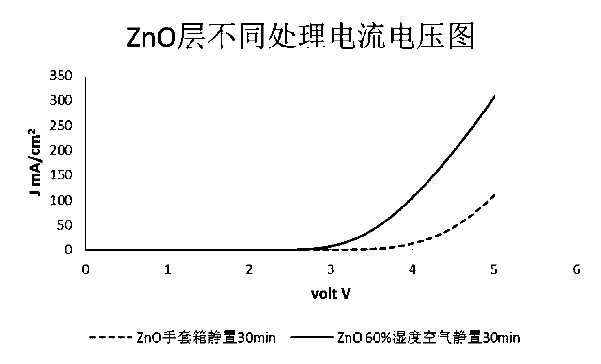
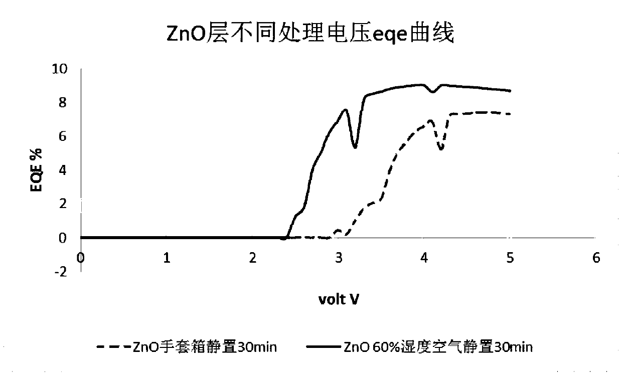
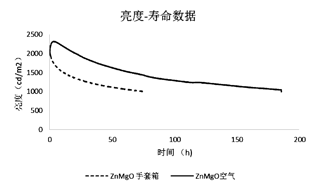
[0020] The invention provides a method for preparing a zinc oxide nanocrystal electron transport layer. After the zinc oxide nanocrystal solution is coated, the electron transport layer is prepared by standing in an environment with a humidity greater than 0% for a period of time.
[0021] In the prior art, when preparing the zinc oxide nanocrystal electron transport layer, it is usually placed at a relatively high temperature for annealing after the zinc oxide nanocrystal solution is coated. However, in the present invention, after the zinc oxide nanocrystal solution is coated, no annealing step is required, but the zinc oxide nanocrystal coating is left to stand for a period of time in an environment with a certain humidity, and the zinc oxide nanocrystal film slows down under the action of water vapor. Crystallization is conducive to improving the conductivity of the film layer and enhancing electron injection, thereby reducing the turn-on voltage of related electronic devic...
Embodiment 1
[0034] QLED positive device preparation:
[0035] S1.ITO glass cleaning
[0036] Put the ITO glass sheet with the number engraved on the back into a glass dish filled with ethanol solution, scrub the ITO surface with a cotton swab, and then use acetone, deionized water, and ethanol to sonicate for 10 minutes respectively, and blow dry with a nitrogen gun. Finally, Place the cleaned ITO glass sheet in oxygen plasma and continue cleaning for 10 minutes;
[0037] S2. Preparation of hole injection layer (Pedot:PSS)
[0038] The cleaned ITO glass sheet was spin-coated with Pedot:PSS in the air, the rotation speed was 3000r / min, and the spin-coating time was 45 seconds. After the spin-coating was completed, it was placed in the air for annealing. The annealing temperature was 150°C, and the annealing time was 30 minutes. After the annealing is completed, quickly transfer the sheet to a glove box with a nitrogen atmosphere;
[0039] S3. Hole transport layer (HTL) preparation
[0...
Embodiment 2
[0048] QLED positive device preparation:
[0049] Cleaning of S1.ITO glass: same as step S1 of embodiment 1;
[0050] S2. Preparation of hole injection layer (Pedot:PSS): same as step S2 of Example 1;
[0051] S3. Hole transport layer (HTL) preparation: same as step S3 of embodiment 1;
[0052] S4. Quantum dot luminescent layer (QDs) preparation: same as step S4 of embodiment 1;
[0053] S5. Preparation of electron transport layer: the sheet obtained in step S4 is spin-coated with zinc oxide nanocrystal solution (30mg / mL, solvent is ethanol) doped with Mg and surface modified with carboxylate ligands at a speed of 2000r / min, and spin-coated 45 seconds, and then leave the sheet in air with a humidity of 90% for 10 minutes;
[0054] S6. Electrode preparation: same as step S6 of Example 1.
PUM
 Abstract
Description
Claims
Application Information
 - R&D
- Intellectual Property
- Life Sciences
- Materials
- Tech Scout
- Unparalleled Data Quality
- Higher Quality Content
- 60% Fewer Hallucinations
Browse by: Latest US Patents, China's latest patents, Technical Efficacy Thesaurus, Application Domain, Technology Topic, Popular Technical Reports.
© 2025 PatSnap. All rights reserved.Legal|Privacy policy|Modern Slavery Act Transparency Statement|Sitemap|About US| Contact US: help@patsnap.com