Wear-resistant pvd tool coating containing tialn nanolayer film
A coating cutting tool and coating technology, applied in the field of metal cutting tools, can solve the problems of high surface roughness and trouble of the deposited layer
- Summary
- Abstract
- Description
- Claims
- Application Information
AI Technical Summary
Problems solved by technology
Method used
Image
Examples
Embodiment 1
[0081] Example 1 - Deposition of coatings according to the invention and comparative coatings
[0082] In the examples and comparative examples of producing cutting tools according to the present invention as follows, a cemented carbide cutting tool substrate body (composition: 12% by weight of Co, 1.6% by weight of (Ta, Nb) C, the rest are WC; WC grain size: 1.5 μm; geometry: ADMT160608R-F56) for coating. The measured residual stress at the substrate surface prior to heating in the deposition chamber was +200 MPa, ie low tensile residual stress.
[0083] Prior to deposition, the substrate body was pretreated by ultrasonic cleaning in ethanol and plasma cleaning. Vacuum the PVD reactor to 8 × 10 -5 mbar, and pretreat the substrate at 550°C.
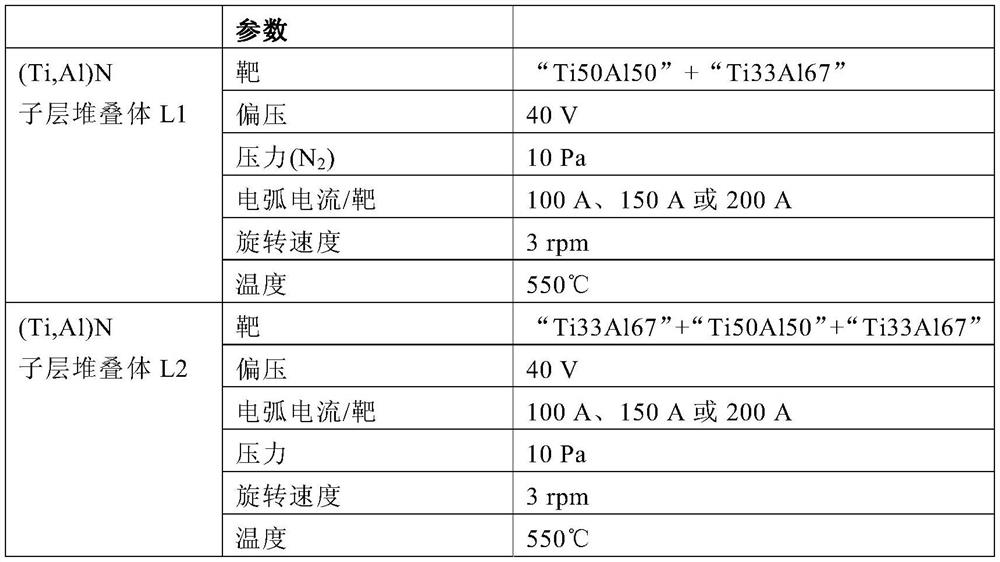
[0084] To deposit (Ti,Al)N coatings, two types of targets with different atomic ratios Ti:Al were used to fabricate alternately stacked (Ti,Al)N sublayers, which The sublayers differ in the atomic ratio Ti:Al: "Ti50Al50" (Ti:Al=50:50)...
Embodiment 2
[0088] Example 2 - Residual Stress, Hardness and Young's Modulus
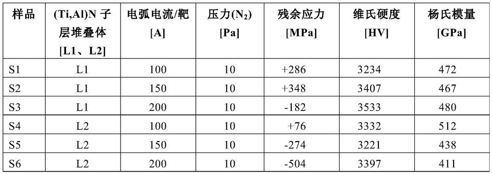
[0089] For the (Ti,Al)N sublayer stacks L1 and L2 deposited according to Example 1, residual stress, hardness and Young's modulus were measured as described above. Because the parameters during the deposition of the individual (Ti,Al)N sublayer stacks L1 or L2, respectively, remain constant, the residual stress in the individual (Ti,Al)N sublayer stacks is constant, but due to the different composition And depending on the arc current applied, the individual layer stacks differ from one another. As described above, each (Ti,Al)N sublayer stack L1 and L2 is respectively deposited directly on the surface of the substrate. The thickness of the layer stack is approximately 2 to 4 μm. The results are shown in Table 2 below.
[0090] Table 2:
[0091]
[0092] The results show that the applied arc current has an effect on the residual stress of the deposited (Ti,Al)N sublayer stack, which also depends on the c...
Embodiment 3
[0095] Example 3 - Surface Roughness
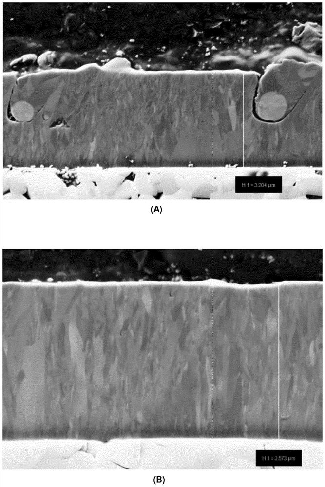
[0096] In order to compare the effect of nitrogen pressure during deposition, two (Ti,Al)N sublayer stacks of L2 type were deposited at 4Pa and 10Pa, respectively, and the surface roughness was measured. The results are shown in Table 2 below. The SEM cross-section of the sample is shown in figure 1 middle. It can be clearly seen that the samples deposited under 4Pa ( figure 1 A) Compared with the sample deposited under 10Pa ( figure 1 B) shows larger droplets. Consequently, the samples deposited at 10 Pa exhibited a much smoother surface roughness. It has been observed that smoother surfaces with fewer droplets and defects are generally obtained if higher pressures are applied during deposition.
[0097] table 3:
[0098]
[0099] Example 4 - cutting test
[0100] In order to evaluate the effect of the coating according to the invention, multilayer coated cutting tools were manufactured and tested in milling tests with respect...
PUM
| Property | Measurement | Unit |
|---|---|---|
| current | aaaaa | aaaaa |
| hardness | aaaaa | aaaaa |
| current | aaaaa | aaaaa |
Abstract
Description
Claims
Application Information


