White-light LED based on perovskite electroluminescence and preparation method thereof
A perovskite, electroluminescence technology, applied in circuits, electrical components, electric solid devices, etc., can solve the problems of blue perovskite material shortage, limited development, low efficiency, etc., to avoid relatively low efficiency and avoid resources. Shortage, Solvent Solvent Erosion Effect
- Summary
- Abstract
- Description
- Claims
- Application Information
AI Technical Summary
Problems solved by technology
Method used
Image
Examples
Embodiment 1
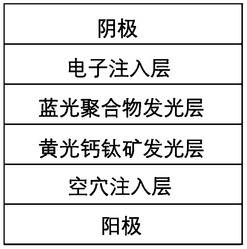
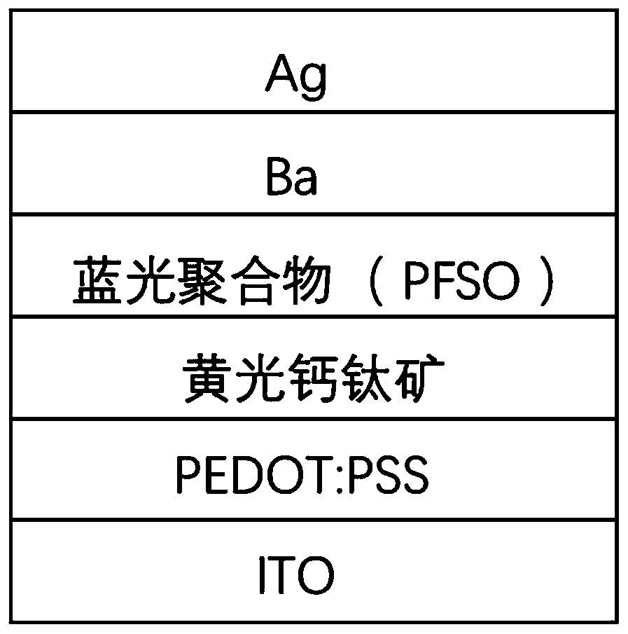
[0053] Such as figure 2 Shown is the structure of the device in this embodiment, from bottom to top: anode (ITO) / hole injection layer (PEDOT:PSS) / yellow light perovskite light-emitting layer (FAPbBr 2.1 I 0.9 ) / blue light polymer light-emitting layer and electron transport layer (PFSO) / electron injection layer (Ba) / cathode (Ag) with emission spectrum peak wavelength of 450nm.
[0054] The preparation process is:
[0055] (1) Put the ITO substrate used in tetrahydrofuran, isopropanol, alkaline cleaning agent and deionized water in sequence for ultrasonic cleaning. The time for ultrasonic cleaning in each liquid is 10 minutes. After the ultrasonic cleaning is completed, the ITO substrate Place it in an oven and dry it for later use; before the hole injection layer (PEDOT:PSS) is spin-coated, the ITO substrate used is subjected to O 2 -Plasma treatment to improve the wettability of PEDOT:PSS on ITO;
[0056](2) A layer of PEDOT:PSS with a thickness of 35nm was deposited as a...
Embodiment 2
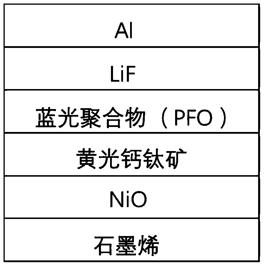
[0061] Such as image 3 Shown is the device structure in the present embodiment, and it is successively from top to bottom: anode (graphene) / hole injection layer (NiO) / emission spectrum peak wavelength is the yellow light perovskite light-emitting layer (MAPbBr) of 580nm 1.8 I 1.2 ) / blue light polymer light-emitting layer and electron transport layer (PFO) / electron injection layer (LiF) / cathode (Al) with emission spectrum peak wavelength of 440nm.
[0062] The preparation process is:
[0063] (1) Place the graphene substrate used in tetrahydrofuran, isopropanol, alkaline cleaning agent and deionized water in sequence for ultrasonic cleaning. The time for ultrasonic cleaning in each liquid is 15 minutes. After the ultrasonic cleaning is completed, the substrate Place in the oven and dry for subsequent use; Before the spin-coated hole injection layer (NiO), the graphene substrate used was subjected to O 2 -Plasma treatment to improve the wettability of NiO on graphene.
[00...
Embodiment 3
[0069] Such as Figure 4 Shown is the device structure of the present embodiment, from top to bottom: anode (ITO) / hole injection layer (CuSCN) / emission spectrum peak wavelength is the yellow light perovskite light-emitting layer (CsPbBr) of 566nm 2.1 I 0.9 ) / blue light polymer light-emitting layer and electron transport layer (G0) / electron injection layer (Ca) / cathode (Al) with emission spectrum peak wavelength of 455nm.
[0070] The preparation process is:
[0071] (1) Put the ITO substrate used in tetrahydrofuran, isopropanol, alkaline cleaning agent and deionized water in sequence for ultrasonic cleaning. The time for ultrasonic cleaning in each liquid is 15 minutes. After the ultrasonic cleaning is completed, the ITO substrate Place it in an oven and dry it for later use; before spin-coating the hole injection layer (CuSCN), the ITO substrate used was subjected to O 2 -Plasma treatment to improve the wettability of NiO on graphene.
[0072] (2) Using a spin-coating pro...
PUM
| Property | Measurement | Unit |
|---|---|---|
| thickness | aaaaa | aaaaa |
| thickness | aaaaa | aaaaa |
Abstract
Description
Claims
Application Information


