Polymer acceptor material
A technology of acceptor materials and polymers, which is applied in the manufacture of electrical solid-state devices, semiconductor devices, semiconductor/solid-state devices, etc., can solve the problems of low device efficiency, achieve strong absorption, improve light-harvesting ability, and broaden the absorption spectrum.
- Summary
- Abstract
- Description
- Claims
- Application Information
AI Technical Summary
Problems solved by technology
Method used
Image

Examples
Embodiment 1
[0029] Example 1: The synthetic route of a representative polymer acceptor material is shown below:
[0030]
[0031] (1) Monomers NDI1 and NDI2 were synthesized according to the method disclosed in the literature (J. Mater. Chem. A, 2017, 5, 5449).
[0032] (2) Monomer PDI1 was synthesized according to the method disclosed in the literature (Macromolecules, 2017, 50, 7559).
[0033] (3) Synthesis of Polymer P1:
[0034] Compound NDI1 (197.0 mg, 0.2 mmol) and compound TN1 (124.8 mg, 0.2 mmol) were weighed into a reaction tube, chlorobenzene (3 mL) was added, and argon gas flowed for 20 minutes. Then quickly add catalyst and ligand, Pd 2 (dba) 3 (3mg), P (o-tol) 3 (6 mg), argon was passed through the reaction tube to fill the reaction tube with argon, the lid was closed, and the polymerization reaction was carried out, and the reaction was carried out at 140° C. for 48 hours. After the reaction is over, drop the reaction solution into methanol to precipitate the polymer...
Embodiment 2
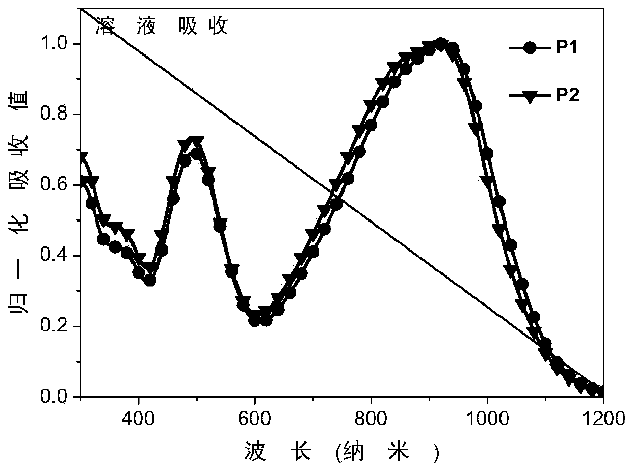
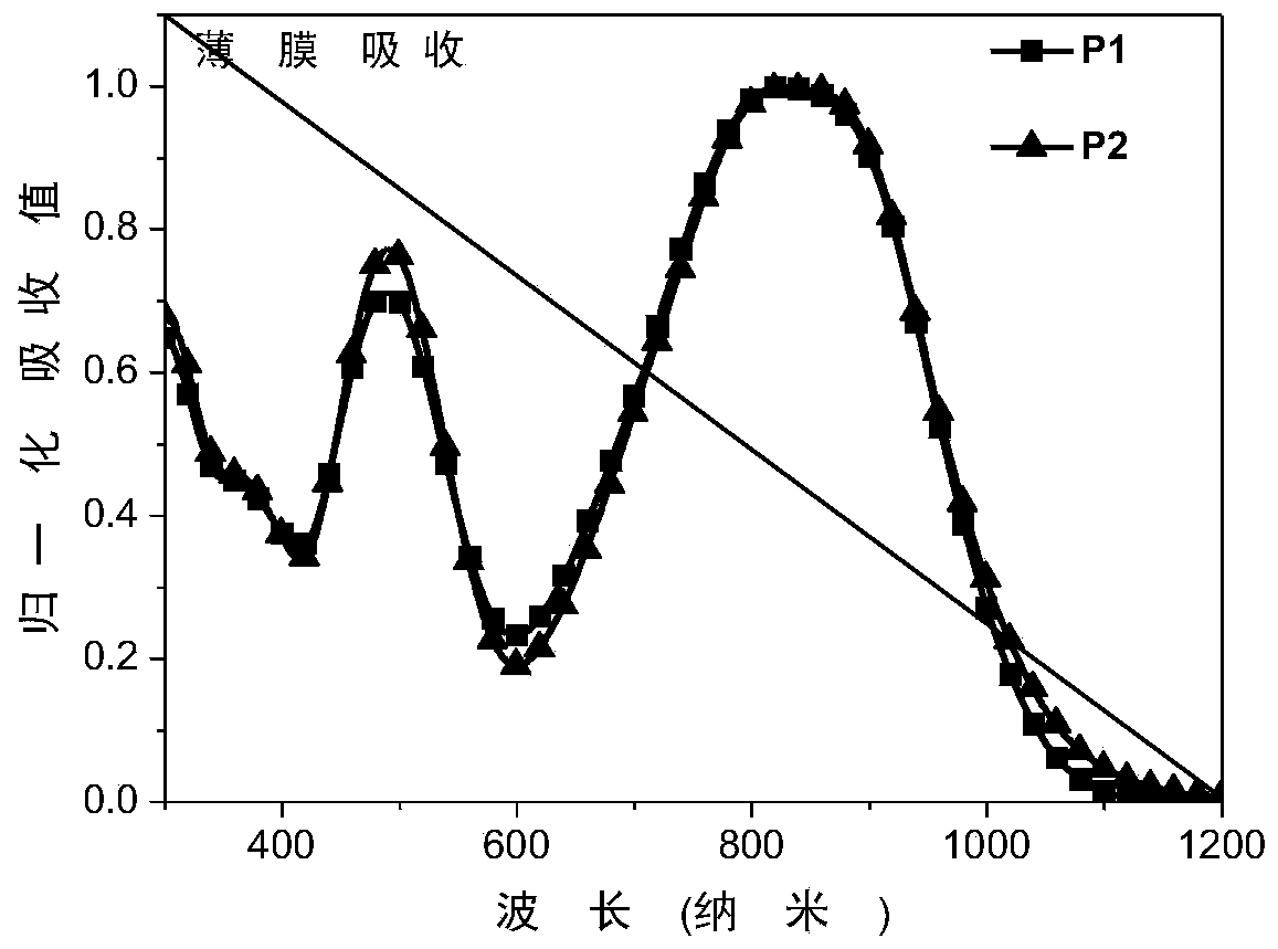
[0043] Example 2: Characterization of organic photovoltaic devices
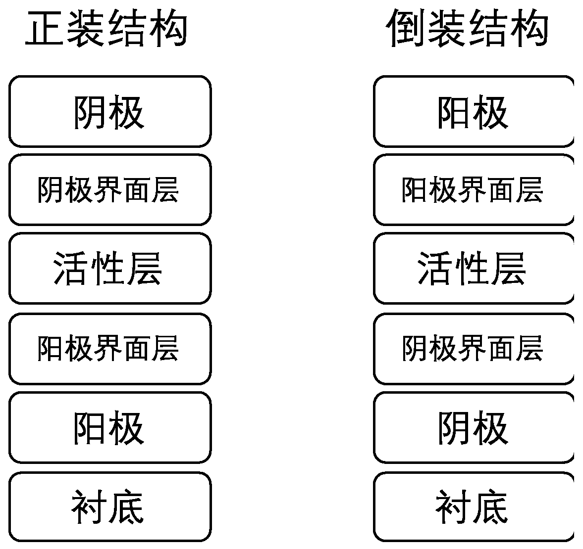
[0044] The representative polymer materials P1 and P2 synthesized in Example 1 are used as electron acceptor materials in organic photovoltaic devices, and the device structure is as follows figure 1 shown.
[0045] The ITO substrate is ultrasonically cleaned in acetone, 1%-3% alkaline cleaning solution, and isopropanol for 20 minutes in sequence, dried in an oven at about 80° C., and plasma treated in a low vacuum. Then, a layer of interfacial layer material is spin-coated on the ITO substrate, and then a layer of active layer material is spin-coated. Then spin-coat a layer of interfacial layer material on the active layer, and finally place the substrate loaded with the active layer in a vacuum thermal evaporation chamber. -6 mbar), metal electrodes were evaporated on the active layer. Organic solar cell devices usually have an energy density of 1000W / m 2 The AM 1.5G was tested and characterized under a...
PUM
| Property | Measurement | Unit |
|---|---|---|
| Optical bandgap | aaaaa | aaaaa |
| Short circuit current density | aaaaa | aaaaa |
Abstract
Description
Claims
Application Information