Transistor with embedded source and drain and preparation method of transistor

A transistor and embedded technology, applied in semiconductor/solid-state device manufacturing, semiconductor devices, electrical components, etc., can solve the problems of reducing the effective drive current of the device, the influence of overlay errors, and reducing the integration density, achieving small device size, high Pressure resistance, small size effect

Pending Publication Date: 2020-04-28
SOUTH UNIVERSITY OF SCIENCE AND TECHNOLOGY OF CHINA
View PDF46 Cites 0 Cited by
  • Summary
  • Abstract
  • Description
  • Claims
  • Application Information

AI Technical Summary

Problems solved by technology

However, LDMOS has some shortcomings that need to be overcome
Due to the introduction of a longer drift region, the size of the device becomes larger and the integration density is reduced
In addition, this drift region introduces a large series resistance, which reduces the effective drive current of the device
In terms of process preparation, since the entire device becomes very asymmetrical, it is difficult to form the drain with a self-aligned process method, and it is easily affected by the overlay error of lithography.

Method used


Image

  • Transistor with embedded source and drain and preparation method of transistor
  • Transistor with embedded source and drain and preparation method of transistor
  • Transistor with embedded source and drain and preparation method of transistor

Examples


Embodiment 1

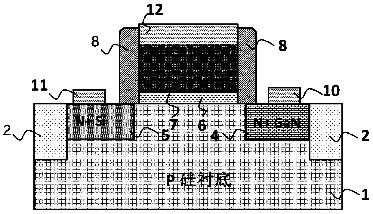
[0041] Embodiment 1 This embodiment provides a high withstand voltage field effect transistor with embedded source and drain

[0042] Such as figure 1Shown is a schematic diagram of the transistor structure, including a weakly p-type doped silicon substrate 1; trench isolation regions 2 embedded in both ends of the silicon substrate 1, and the upper surface of the trench isolation region 2 is in contact with the silicon substrate The upper surface of the bottom 1 is coplanar; the heavily N-type doped drain 4 and the heavily N-type doped source 5 embedded near both ends of the silicon substrate 1; the heavily N-type doped drain 4 The heavily N-type doped source 5 is in contact with the trench isolation region 2, and the heavily N-type doped drain 4 and the heavily N-type doped source 5 top surfaces are in contact with the silicon substrate 1 top surface Coplanar; the gate oxide layer 6 on the silicon substrate 1; the gate 7 on the gate oxide 6; the gate contact 12 on the gate ...

Embodiment 2

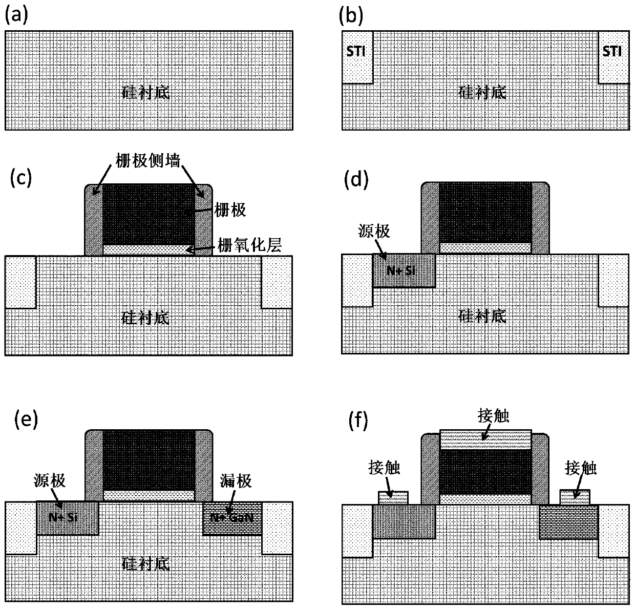
[0053] Embodiment 2 This embodiment provides a novel method for manufacturing a high withstand voltage field effect transistor with embedded source and drain

[0054] Such as image 3 (a) The schematic structure of the transistor shown in (a), the initial bulk silicon substrate is selected, and the substrate is doped with weak p-type doping, and the doping concentration is 10 17 cm -2 , the substrate is a silicon-based material deposited on an insulating layer.

[0055] Chemical vapor deposition of a layer of aluminum oxide gate oxide layer with a thickness of 10nm and a layer of polysilicon positive gate with a thickness of 100nm; photolithography and open the window of the positive gate pattern, and then use photoresist as a mask to align the positive gate The gate is dry etched to form a pattern of the gate, and KOH solution is used for wet etching.

[0056] Atomic layer deposition of a layer of low dielectric constant dielectric SiOCN as the gate spacer material, follow...


PUM

PropertyMeasurementUnit
thicknessaaaaaaaaaa
thicknessaaaaaaaaaa
thicknessaaaaaaaaaa

Abstract

The invention provides a transistor with embedded source and drain and a preparation method of the transistor The transistor structurally comprises a weak p-type doped silicon substrate 1, trench isolation regions 2 embedded into the two end parts of the silicon substrate 1, a heavy N-type doped drain 4 and a heavy N-type doped source 5 embedded into the vicinity of the two end parts of the silicon substrate 1 respectively, a gate oxide layer 6 positioned on the silicon substrate 1, a grid electrode 7 positioned on the gate oxide layer 6, a gate contact 12 on the gate 7, and a side wall 8 positioned on the side surface of the grid 7. Embedded gallium nitride is introduced into the drain electrode, and the withstand voltage of the transistor is greatly improved by means of the wide bandgapcharacteristic of gallium nitride. Compared with the traditional silicon-based field effect transistor, the novel transistor provided by the invention has a similar symmetrical structure, does not need a channel region without grid coverage, and has the advantages of small device size, small on-resistance and complete compatibility with a self-alignment process.

Description

technical field [0001] The invention belongs to the technical field of integrated circuits and semiconductor devices, and in particular relates to a transistor with embedded source and drain and a preparation method thereof. Background technique [0002] Integrated circuit technology is the cornerstone of the development of contemporary information society. Since the invention of the first integrated circuit with only five components in the 1950s, the integrated circuit has developed rapidly towards the trend of multi-function, high speed, low power consumption and low price, and has become an indispensable part of various information technologies. Core components. The driving force behind the rapid development of integrated circuits is the continuous reduction in the size of unit field effect transistors. In large-scale digital integrated circuits and low-power analog integrated circuits, field effect transistors generally have low operating voltages to achieve low power ...

Claims


Application Information

Patent Timeline
Patent Type & Authority Applications(China)
IPC IPC(8): H01L29/08H01L29/20H01L29/06H01L29/78H01L21/336
CPCH01L29/7816H01L29/66681H01L29/0856H01L29/0873H01L29/0615H01L29/2003
Inventor 刘冉万景叶怀宇张国旗
Owner SOUTH UNIVERSITY OF SCIENCE AND TECHNOLOGY OF CHINA
Why Eureka
Try Eureka