Method for manufacturing grating nano-imprinting template by using electron beam lithography technology

A technology of electron beam lithography and nano-imprinting, applied in microlithography exposure equipment, diffraction gratings, optics, etc., can solve the problems of insufficient emphasis, long template processing time, and inability to achieve, prolong service life and save energy. Material and time, the effect of increasing size

Inactive Publication Date: 2020-05-15
SHENZHEN LOCHN OPTICS TECH CO LTD
View PDF4 Cites 5 Cited by
  • Summary
  • Abstract
  • Description
  • Claims
  • Application Information

AI Technical Summary

Problems solved by technology

In the existing technical solutions, hard materials such as silicon and quartz glass are usually used as the substrate material, and the photoresist spin-coated on the hard substrate is subjected to photolithographic exposure through a mask, and then developed to obtain the desired Structure, or mechanical scribing method, electron beam direct writing exposure, laser direct writing exposure, laser interference exposure, so the template processing time is long, the cost is high, and the price is expensive
[0003] The production of grating templates in the prior art has the following disadvantages: 1. Using the imprint template made by exposing the photoresist requires a

Method used


Image

  • Method for manufacturing grating nano-imprinting template by using electron beam lithography technology
  • Method for manufacturing grating nano-imprinting template by using electron beam lithography technology

Examples


Embodiment Construction

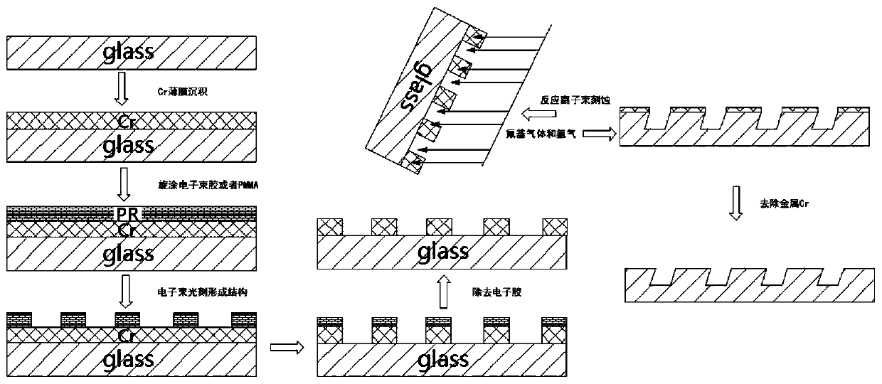
[0020] see figure 1 As shown, the technical solution adopted in this embodiment is:

[0021] S1: Using Auto CAD or electron beam lithography design software to design the nanostructure grating;

[0022] S2: Deposit metal materials on silicon or quartz substrates by means of magnetron sputtering or ion beam deposition;

[0023] S3: Use spin coating technology to uniformly cover a certain amount of electron beam glue or PMMA material on the metal film to form a uniform organic polymer film

[0024] S4: The substrate coated with electron beam glue or PMMA material is completely dried in an oven, and then cooled after drying;

[0025] S5: Transmit the grating design drawing to the instrument for identification and parameter setting;

[0026] S6: Adjust the voltage required for electron beam lithography according to the thickness and characteristics of the electron beam glue;

[0027] S7: Using electron beam lithography to engrave the structure on the electron glue or PMMA film...


PUM

PropertyMeasurementUnit
Thicknessaaaaaaaaaa

Abstract

The invention discloses a method for manufacturing a grating nano-imprinting template by using an electron beam lithography technology, and relates to a method for manufacturing a nano-imprinting template on silicon or glass by using electron beam lithography in combination with inductive coupling plasma etching and reactive ion beam etching technologies. The invention aims to improve the manufacturing process of a template to a nanoscale, improve the stability of the template and the uniformity of a nanostructure, and improve the imprinting quality and precision.

Description

technical field [0001] The invention relates to the technical field of grating nano-imprint templates, in particular to a method for making grating nano-imprint templates using electron beam lithography technology. Background technique [0002] Since nanoimprint technology was proposed in the last century, it is considered to be one of the most promising nano-device manufacturing technologies, which provides the possibility of low-cost manufacturing of large-scale, highly ordered nano-device arrays. At present, due to the uniqueness of this technology, it is also widely used in the research and development of optical devices. In the process of nanoimprinting, the production of the template is the core, and the quality of the template will directly affect the integrity and uniformity of the imprinted structure. In the existing technical solutions, hard materials such as silicon and quartz glass are usually used as the substrate material, and the photoresist spin-coated on th...

Claims


Application Information

Patent Timeline
IPC IPC(8): G02B5/18G03F7/16G03F7/20
CPCG02B5/1857G03F7/162G03F7/168G03F7/2059
Inventor 马国斌宋强赵朔汪涛
Owner SHENZHEN LOCHN OPTICS TECH CO LTD
Why Eureka
Try Eureka