Method for improving infrared band transmittance by processing micro-nano structure on surface of chalcogenide glass

A chalcogenide glass, micro-nano structure technology, applied in optical components, optics, instruments, etc., can solve the problems of unsuitable scale three-dimensional structure, only suitable for, unable to control the microstructure morphology, etc., to solve the problem of film quality, The effect of avoiding contact damage and good anti-reflection micro-nano structure stability

Active Publication Date: 2020-05-19
BEIJING INSTITUTE OF TECHNOLOGYGY +1
View PDF3 Cites 5 Cited by
  • Summary
  • Abstract
  • Description
  • Claims
  • Application Information

AI Technical Summary

Problems solved by technology

Although this microstructure processing method can realize microstructure processing on the surface of chalcogenide glass, it also has disadvantages: using mechanical stamping, the hardness of the template is higher than that of chalcogenide glass, and deformation and stress will occur on the entire processed surface; It is necessary to heat the chalcogenide glass above its glass transition temperature, and the molding process is carried out at high temperature; the components of the chalcogenide glass

Method used


Image

  • Method for improving infrared band transmittance by processing micro-nano structure on surface of chalcogenide glass
  • Method for improving infrared band transmittance by processing micro-nano structure on surface of chalcogenide glass
  • Method for improving infrared band transmittance by processing micro-nano structure on surface of chalcogenide glass

Examples


Embodiment 1

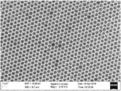
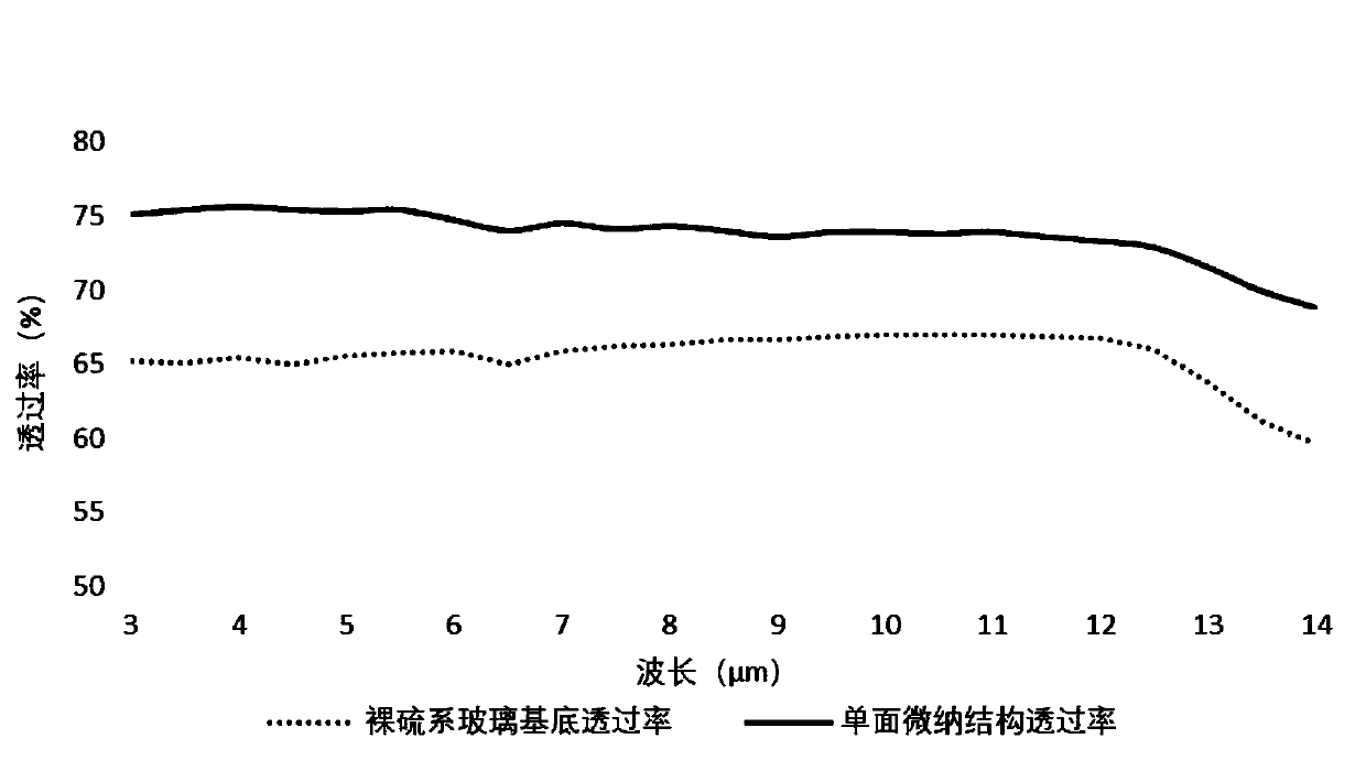
[0027] For the chalcogenide glass As40Se60 (As40Se60, Joint Research Center of Chengdu University of Information Technology & Chengdu Lansun Optoelectronics Technology Co., Ltd.), a regularly arranged three-dimensional bowl-shaped micro-nano structure is designed to achieve 3 μm ~ 12 μm broadband anti-reflection, specifically The processing process is as follows:

[0028] (1) On the surface of the chalcogenide glass As40Se60, apply a coating of ultraviolet imprinting glue (code name 04n, Obducat micro-nano imprinting company) with a thickness of 100nm in a glue-spinning manner;

[0029] (2) Use the SiC printing plate engraved with the target pattern (arranged by three-dimensional bowl-shaped structural units, consistent with the micro-nano structure etched on the surface of the chalcogenide glass As40Se60) to imprint the polyethylene (PE) transfer template, first in Heat at 155°C for 100s, then cool down to 100°C and hold for 90s, then cool down to 90°C, transfer the target pa...


PUM

PropertyMeasurementUnit
Thicknessaaaaaaaaaa

Abstract

The invention relates to a method for improving infrared band transmittance by processing a micro-nano structure on a surface of chalcogenide glass, and belongs to the technical field of infrared optical glass processing and application. According to the method, the micro-nano structure with a proper refractive index is directly manufactured on the surface of the chalcogenide glass, introduction of a new film material is avoided, and problems that a multi-layer film material is limited and quality of a film layer is poor in a traditional infrared antireflection film plating process are solved;reactive ion etching adopted in the method is mainly based on a chemical reaction of a gas and the chalcogenide glass, does not generate any effect on a part covered by a polymer coating, avoids generation of a stress, is performed at a normal temperature and in a vacuum state, and does not generate gasification and leakage of toxic components; and according to the method, micro-nano structure pattern impressing of a non-planar surface can be achieved, a category of large-area micro-nano machining optical elements is expanded, and efficient antireflection of the chalcogenide glass in all infrared wave bands can be achieved by changing a target graphic structure and technological parameters.

Description

technical field [0001] The invention specifically relates to a method for processing three-dimensionally arranged micro-nano structures on the surface of chalcogenide glass to improve the transmittance in the infrared band, and belongs to the technical field of infrared optical glass processing and application. Background technique [0002] Chalcogenide glass is a binary or ternary compound glass composed of sulfur, selenium, tellurium and other glass network bodies (such as arsenic, antimony, germanium, etc.). In the 1950s and 1960s, arsenic sulfide glass was mass-produced by several companies in the United States, the United Kingdom, and Europe, and was used as a mid-infrared window material of 3 μm to 5 μm. At the same time, the concept and technology of infrared thermal imaging gradually emerged, making people shift the focus to the research of chalcogenide glass that transmits longer wavelength bands. Afterwards, selenide and telluride chalcogenide glasses, which can t...

Claims


Application Information

Patent Timeline
IPC IPC(8): G02B1/118
CPCG02B1/118
Inventor 王岭雪程海娟蔡毅李茂忠孟令海吴绍华木锐黄攀贾钰超钟海政
Owner BEIJING INSTITUTE OF TECHNOLOGYGY
Why Eureka
Try Eureka