High-frequency narrow-pulse semiconductor laser driving circuit

A driving circuit and narrow pulse technology, which is applied in the field of high-frequency narrow pulse semiconductor laser driving circuit, can solve the problems that the pulse transformer cannot meet the narrow pulse output, the rise time and fall time are too large, and the single pulse signal is susceptible to interference, etc., to achieve The maintenance and replacement of components is convenient, the accuracy is maintained, and the effect of improving anti-interference ability

Pending Publication Date: 2020-05-26
YUYAO SUNNY OPTICAL INTELLIGENCE TECH CO LTD
View PDF3 Cites 3 Cited by
  • Summary
  • Abstract
  • Description
  • Claims
  • Application Information

AI Technical Summary

Problems solved by technology

For example, the patent literature with the publication number CN101009486A pointed out "Insulated Gate Power Transistor Narrow Pulse Driver". Turn off, although the shaping of the pulse signal can also be realized, the pulse transformer cannot meet the higher requirements of the narrow pulse output, and the design of the pulse signal connected to the gate of the power transistor T is also prone to the problem of excessive rise time and fall time , single-pulse signals are susceptible to interference, and the circuit stability is not high, so the above-mentioned circuit can never be driven by a narrow pulse with a pulse width less than 1 ns; another example is a patent document with the announcement number CN103227413B disclosing a "semiconductor laser drive circuit", Including: a pulse shaping circuit, used to shape the waveform of the input narrow pulse signal, and further compress its pulse width; and a power amplifier circuit, connected with the pulse shaping circuit, used to use high voltage to adjust the output narrow pulse The pulse signal is power amplified, and the high level of the amplified narrow pulse signal is output to the positive pole of the laser, and the low level is output to the negative pole of the laser
It can meet the requirements of high power and narrow pulse at the same time, and finally debug and obtain a signal with a pulse width as narrow as 20ns and a repetition frequency range of 100Hz-100KHz, but it is relatively difficult to adjust a narrow pulse with a pulse width less than 1ns

Method used


Image

  • High-frequency narrow-pulse semiconductor laser driving circuit
  • High-frequency narrow-pulse semiconductor laser driving circuit
  • High-frequency narrow-pulse semiconductor laser driving circuit

Examples


Embodiment 1

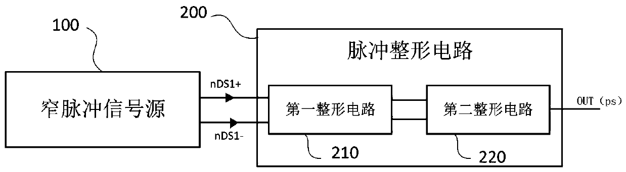
[0043] Such as figure 1 As shown, this embodiment provides a high-frequency narrow-pulse semiconductor laser drive circuit, including:

[0044] The narrow pulse signal source 100 is used to output a pair of nanosecond level differential narrow pulse signals. The nanosecond level refers to the pulse width of the pulse signal as nanosecond level; The signal output terminals are respectively connected with an output signal line, one signal line transmits the positive signal of the nanosecond differential narrow pulse signal, and one signal line transmits the negative signal of the nanosecond differential narrow pulse signal. The amplitude of the two signals is equal, the phase difference is 180 degrees, and the polarity is opposite. The traces of the two signal lines on the PCB are equal in length, equal in width, close together, and on the same level; as we all know, the inherent advantages of differential transmission signals are Strong anti-interference ability, can effective...

Embodiment 2

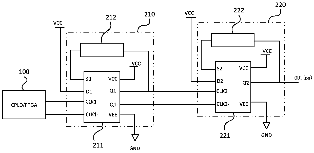
[0054] Such as image 3 As shown, the difference between this embodiment and Embodiment 1 is that in the semiconductor laser drive circuit of this embodiment, the first shaping circuit 210 includes a first flip-flop 211 and a first delay circuit 212; the first trigger The data input terminal D1 of the flip-flop 211 is connected to an external power supply, and the first and second clock input terminals (CLK1, CLK1-) of the first flip-flop 211 are respectively used as the first and second clocks of the first shaping circuit 210 Signal input end, the first output end Q1 of the first flip-flop 211 is connected to the input end of the first delay circuit 212 and serves as the first output end of the first shaping circuit 210, the first flip-flop The second output terminal Q1 of 211-is the second output terminal of the first shaping circuit 210, and the reset input terminal R1 of the first flip-flop 211 is connected to the output terminal of the first delay circuit 212;

[0055] T...


PUM


Abstract

The invention relates to the technical field of semiconductor lasers, and discloses a high-frequency narrow-pulse semiconductor laser driving circuit. The driving circuit comprises a narrow-pulse signal source and a pulse shaping circuit, wherein the narrow-pulse signal source is used for outputting a pair of nanosecond differential narrow-pulse signals; and the pulse shaping circuit is connectedwith the narrow pulse signal source and is used for triggering shaping of the differential narrow pulse signal according to the edge of the differential narrow pulse signal and outputting a path of picosecond-level narrow pulse signals. According to the invention, two paths of nanosecond-level narrow pulse signals are transmitted at the same time by utilizing a differential signal concept, so thatthe signal transmission process has relatively strong anti-interference capability; the pulse widths of the two paths of nanosecond-level narrow pulse signals are respectively shaped and compressed through the pulse shaping circuit; and finally, one path of picosecond-level narrow pulse signals is output, so that the requirement for obtaining narrower pulses in laser driving application is met, external interference in the nanosecond-level narrow pulse signal transmission process can be prevented through application of edge triggering, and the correctness of transmitted data is guaranteed.

Description

technical field [0001] The invention relates to the technical field of semiconductor lasers, in particular to a high-frequency narrow-pulse semiconductor laser drive circuit. Background technique [0002] Semiconductor lasers are gradually replacing He-Ne lasers in many aspects, and have been widely used in optical fiber communications, integrated optics, laser printing, laser beam scanning, optical disk storage technology, laser ranging, laser radar, pumped solid-state lasers, pulse Doppler Le imaging, 3D image system, fiber optic temperature sensor and other fields. In many fields, especially in the fields of target recognition and laser ranging, the performance of target recognition, ranging accuracy, anti-interference and low power consumption all depend on the quality of laser pulses emitted by semiconductor lasers, and semiconductor lasers The emitted optical pulse is directly modulated by the electrical pulse generated by the semiconductor laser drive circuit, that i...

Claims


Application Information

Patent Timeline
Patent Type & Authority Applications(China)
IPC IPC(8): H01S5/042
CPCH01S5/0428
Inventor 陈华钧徐杰伟李大猛
Owner YUYAO SUNNY OPTICAL INTELLIGENCE TECH CO LTD
Why Eureka
Try Eureka