Anodic bonding method

An anodic bonding and bonding technology, applied in precision positioning equipment, microstructure technology, microstructure devices, etc., can solve problems such as easy introduction of impurities, adverse effects on MEMS device performance, and long process time

Active Publication Date: 2020-06-02
KUNSHAN BRANCH INST OF MICROELECTRONICS OF CHINESE ACADEMY OF SCI
View PDF13 Cites 0 Cited by
  • Summary
  • Abstract
  • Description
  • Claims
  • Application Information

AI Technical Summary

Problems solved by technology

At present, the wafer bonding technology mainly includes anodic bonding, silicon wafer direct bonding, eutectic bonding, thermocompression bonding, metal bonding, glass solder bonding, etc. The above wafer bonding technologies all involve high temperature annealing Processing, the process time is long, and the high temperature generated during the bonding process will adversely affect the performance of MEMS devices. For example, high temperature will cause thermal damage to the temperature-sensitive circuits and microstructures on the wafer; high temperature is easy to introduce impurities, resulting in substrate doping redistribution; for wafers and metals with large differences in thermal expansion coefficients, high temperature treatment will lead to large deformation and residual thermal stress, which directly affects device performance and packaging yield

Method used


Image

  • Anodic bonding method
  • Anodic bonding method
  • Anodic bonding method

Examples


Embodiment Construction

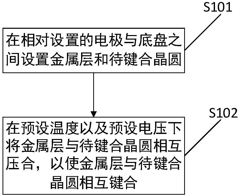
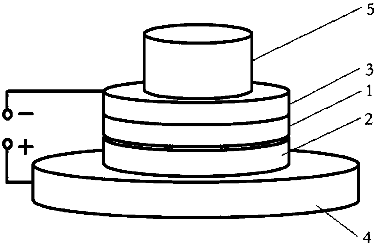
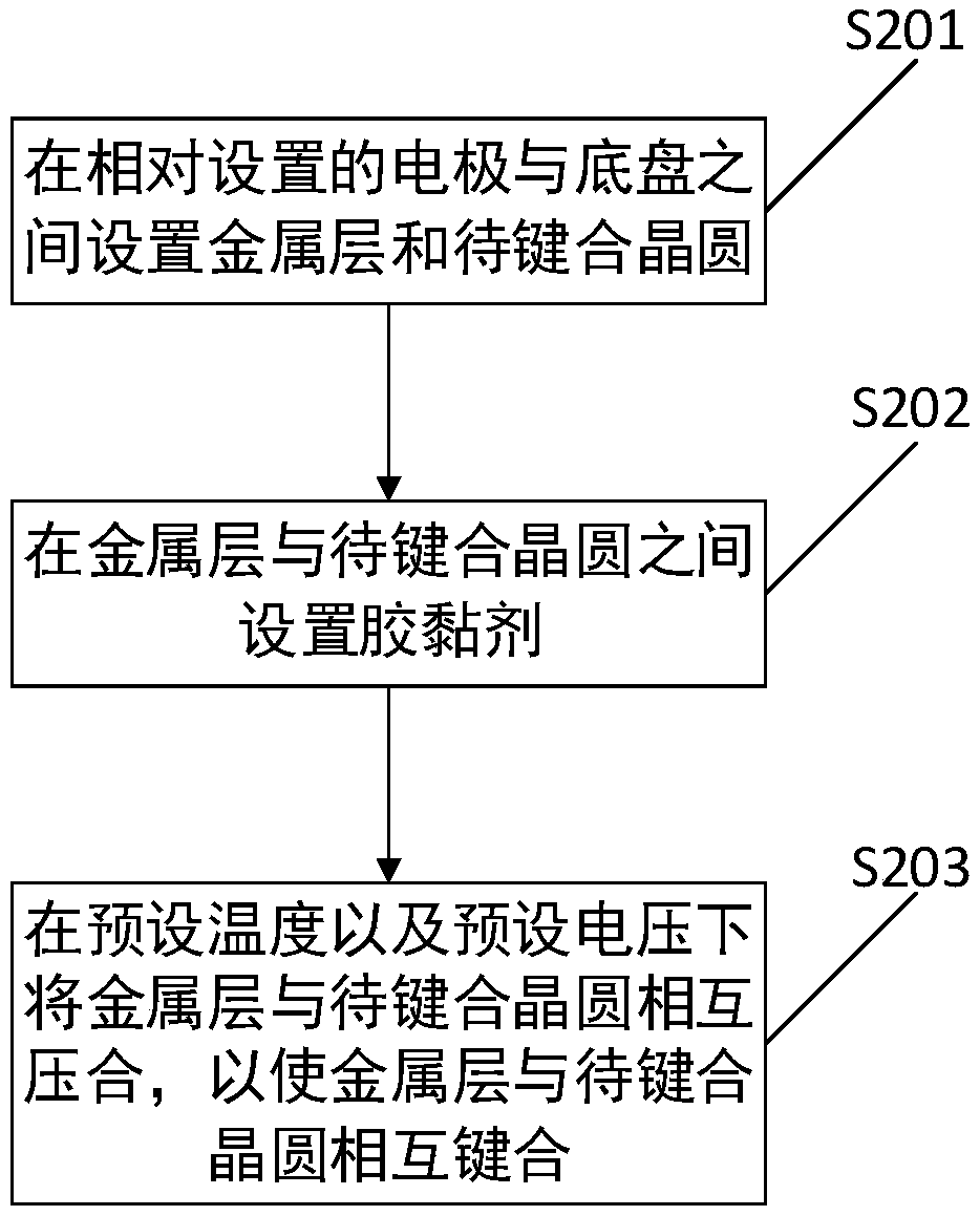
[0026] The core of the present invention is to provide an anodic bonding method. In the prior art, when anodic bonding is performed, the surface activity between the wafer and the metal layer is usually increased by means of high temperature, so as to realize the bonding between the wafer and the metal layer. However, the high temperature generated during the bonding process will adversely affect the performance of MEMS devices. For example, high temperature will cause thermal damage to the temperature-sensitive circuits and microstructures on the wafer; high temperature is easy to introduce impurities, resulting in redistribution of substrate doping; for Wafers and metal layers with large differences in thermal expansion coefficients will cause large deformation and residual thermal stress after high temperature treatment, which directly affects device performance and packaging yield.

[0027] In the anodic bonding method provided by the present invention, the metal layer wil...


PUM

PropertyMeasurementUnit
thicknessaaaaaaaaaa

Abstract

The invention discloses an anodic bonding method, which comprises the following steps of: a metal layer contacts with an electrode during bonding, and the electrode is electrically connected with a positive electrode of a direct-current power supply; the wafer to be bonded is contacted with the chassis, and meanwhile, the chassis is electrically connected with the negative electrode of the direct-current power supply. In the bonding process, a preset voltage is applied between the electrode and the chassis through the direct-current power supply to form an electric field, so that the metal layer and the wafer to be bonded are located in the electric field. The electric field can accelerate the bonding process by accelerating the reaction rate between the wafer to be bonded and the metal layer and the like, so that the temperature required by anodic bonding can be effectively reduced.

Description

technical field [0001] The invention relates to the field of integrated circuit preparation, in particular to an anode bonding method. Background technique [0002] With the development of integrated circuits, silicon-on-insulator (SOI) technology is recognized by the industry as one of the solutions to replace the existing monocrystalline silicon materials in the era of nanotechnology, and it is a powerful tool to maintain the trend of Moore's Law. [0003] SOI materials are the basis for the development of SOI technology, and high-quality SOI materials have always been the primary factor restricting SOI technology from entering large-scale industrial production. In recent years, with the continuous maturity of SOI material preparation technology, the material problems that restrict the development of SOI technology are gradually being solved. In the final analysis, the preparation technology of SOI material includes two kinds, that is, the separation-by-oxygen implantatio...

Claims


Application Information

Patent Timeline
Patent Type & Authority Applications(China)
IPC IPC(8): B81C3/00H01L21/60
CPCB81C3/001H01L24/82B81C2203/031H01L2224/82893
Inventor 王盛凯王英辉
Owner KUNSHAN BRANCH INST OF MICROELECTRONICS OF CHINESE ACADEMY OF SCI
Why Eureka
Try Eureka