Self-indicating patch semiconductor laser and packaging method thereof

A packaging method and chip packaging technology, applied in the direction of semiconductor lasers, lasers, laser parts, etc., can solve the problems of affecting stability, equipment failure, high structure, etc., to achieve flattening and miniaturization, and reduce the distance of the optical path. , the effect of prolonging the service life

Inactive Publication Date: 2020-06-02
潍坊华光光电子有限公司
View PDF11 Cites 0 Cited by
  • Summary
  • Abstract
  • Description
  • Claims
  • Application Information

AI Technical Summary

Problems solved by technology

However, the device indicates that the light and the working laser are different lasers, and cannot be powered at the same time, which increases the possibility of malfunction due to circuit failure
[0008] To sum up, in the existing market, especially the lasers used in the market for miniaturization applications, the lasers with indicator light are generally realized by two lasers through optical beam combination. Since the two independent lasers need independent power supply, The working current required by the high-power laser and the indicator laser is inconsistent, and the leakage electrode of the high-power laser is easy to burn the indicator laser, causing equipment failure and affecting stability
Moreover, the packaging form is generally TO packaged lasers, which have a high structure and cannot meet some specific flat requirements; there are also lasers such as LED chip packages, although they meet the flat design, but the light output direction is parallel to the PCB board. , cannot meet the requirements of vertical light output, and this patch type is not as easy to replace as the existing in-line tube socket in later maintenance

Method used


Image

  • Self-indicating patch semiconductor laser and packaging method thereof
  • Self-indicating patch semiconductor laser and packaging method thereof
  • Self-indicating patch semiconductor laser and packaging method thereof

Examples


Embodiment 1

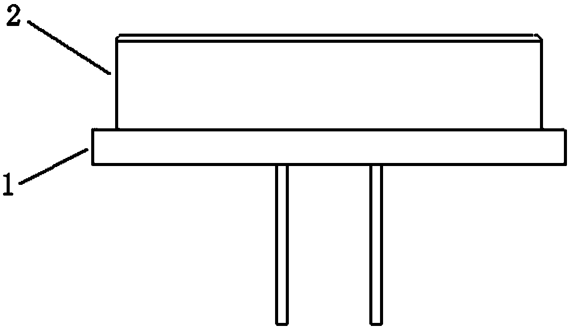
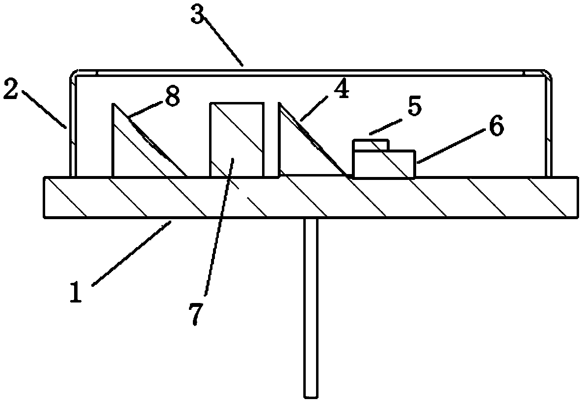
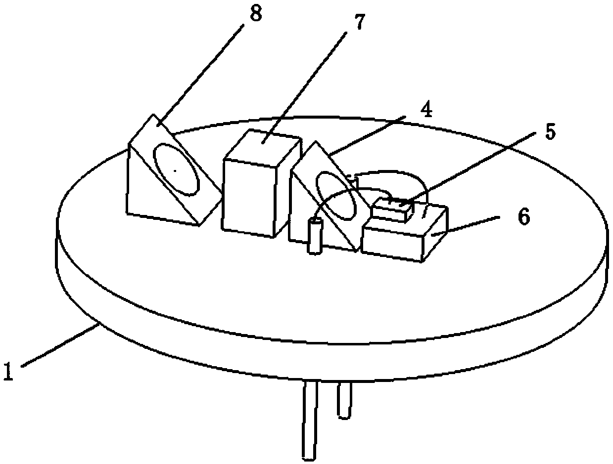
[0051] A self-indicating chip semiconductor laser, including a tube base 1 and a tube cap 2 arranged on the tube base 1, the overall appearance schematic diagram is as follows figure 1 shown. In the space formed by the tube base 1 and the tube cap 2, COS, a 45° right-angle semi-reflection table 4, a crystal 7, and a 45° right-angle total reflection table 8 are sequentially arranged on the tube base 1 along the optical path; the cross-sectional schematic diagram is as follows figure 2 shown. The schematic diagram of the structure before capping is as follows: image 3 shown.

[0052] The 45° right-angle semi-reflective table 4 is coated with an 808nm semi-permeable film on the reflective surface. The transmittance and reflectivity can be adjusted by adjusting the coating, so that 50% of the 808nm laser emitted by the die 5 can be emitted horizontally and 50% of the light can be changed. The light path exits vertically. There is a crystal 7 on the optical path, which makes ...

Embodiment 2

[0054] According to the self-indicating chip semiconductor laser described in Embodiment 1, the difference is that the COS includes a heat sink 6 and a die 5 sintered on the heat sink 6 , and the die 5 is flip-chip mounted on the heat sink 6 . The heat emitted by the tube core 5 can be dissipated faster. The solder used for bonding the die 5 of the laser is gold-tin solder, which has the characteristics of high strength, good oxidation resistance, excellent thermal fatigue and creep resistance, low melting point, and good fluidity. The heat sink 6 is an insulating heat sink. Make the shell uncharged to reduce the probability of electrostatic breakdown of the laser in subsequent applications. The COS parallel patch is on the base 1. The overall vertical height of the laser is reduced by about 2 mm, which makes the structure flat and meets the application of some flat spaces. The material used is silver glue. There is a COS positioning groove on the tube base 1, which is con...

Embodiment 3

[0056] A self-indicating chip semiconductor laser according to embodiment 1 or 2, the difference is that,

[0057] The tube base 1 is different from the ordinary TO tube base. The tube base 1 does not have the tongue of the conventional tube base, which shortens the vertical length of the laser, makes the structure flat, and can adapt to the application of relatively narrow space.

[0058] The crystal 7 is Nd:YVO4 crystal or KTP crystal, and the crystal 7 is fixed on the stem 1 by optical ultraviolet glue. Curing is quick and easy to handle.

[0059] The cap 2 is provided with a coating window 3 . The enhanced transmittance of the laser can be increased. The tube cap 2 is sealed in a nitrogen environment during the packaging process, so that the laser works in an oxygen-free environment to reduce oxidation of the laser, and the airtight space can also prevent dust.

[0060] The material of 45° right-angle semi-reflection table 4 and 45° right-angle total reflection table 8 ...


PUM


Abstract

The invention relates to a self-indicating patch semiconductor laser and a packaging method thereof. The self-indicating patch semiconductor laser comprises a tube socket and a tube cap arranged on the tube socket, and in a space formed by the tube socket and the tube cap, a COS, a 45-degree right-angle semi-reflection table, a crystal and a 45-degree right-angle total reflection table are sequentially arranged on the tube socket along an optical path; two 45-degree reflective modules are arranged on the tube socket; the first 45-degree light reflection module (45-degree right-angle half-reflection table) reflects 50% of laser, so that a light path is changed by 90 degrees, the laser is emitted in a direction vertical to the tube socket, 50% of laser can also pass through the lens, a crystal is arranged on the light path, a 808nm laser is pumped into a 1064nm laser, then the 532nm laser green laser is generated through a frequency doubling crystal, and after the green laser passes through a second 45-degree reflection module (45-degree right-angle total reflection table), the light path is changed by 90 degrees and is emitted out perpendicular to the tube base.

Description

technical field [0001] The invention relates to a self-indicating patch semiconductor laser and a packaging method thereof, belonging to the technical field of packaging and manufacturing of semiconductor lasers. Background technique [0002] Semiconductor lasers have the advantages of small size, light weight, low cost, long life, selectable wavelength, stable output power, and simple power drive system. widely. Semiconductor lasers have the advantages of small size, long life, etc., and can be pumped by a simple way of injecting current. Their operating voltage and current are compatible with integrated circuits, so they can be monolithically integrated with them. Moreover, it is also possible to directly perform current modulation with a frequency up to GHz to obtain high-speed modulated laser output. Due to these advantages, semiconductor diode lasers have been widely used in laser communication, optical storage, optical gyro, laser printing, ranging and radar. In cli...

Claims


Application Information

Patent Timeline
Patent Type & Authority Applications(China)
IPC IPC(8): H01S5/022
CPCH01S5/0225H01S5/023H01S5/0231H01S5/0233H01S5/0235
Inventor 王友志秦华兵尚秀涛郑兆河
Owner 潍坊华光光电子有限公司
Why Eureka
Try Eureka