GaN-based normally-off high-electron-mobility transistor and preparation method thereof

A high electron mobility, normally-off technology, applied in transistors, semiconductor/solid-state device manufacturing, circuits, etc., can solve problems such as device performance impact, etching process damage, and threshold voltage not high enough to achieve good high-frequency performance, The effect of low on-resistance and high threshold voltage

Inactive Publication Date: 2020-06-05
INST OF SEMICONDUCTORS - CHINESE ACAD OF SCI
View PDF7 Cites 0 Cited by
  • Summary
  • Abstract
  • Description
  • Claims
  • Application Information

AI Technical Summary

Problems solved by technology

Each method has its own advantages and disadvantages. For example, fluorine ion treatment is inevitable to avoid implantation damage, groove gate is difficult to avoid etching damage, thin barrier threshold voltage is low, and insufficient 2DEG in the source and drain regions affects the device saturation current and on-state resistance, pn The junction gate is limited by the insufficient hole concentration of p-GaN and the threshold voltage is not high enough
Some research groups have also reported groove-shaped or inclined-plane channel devices. The groove-shaped or inclined-plane channel is formed by etching and then epitaxy, but the etching process inevitably causes certain damage, which has a greater impact on device performance.

Method used


Image

  • GaN-based normally-off high-electron-mobility transistor and preparation method thereof
  • GaN-based normally-off high-electron-mobility transistor and preparation method thereof
  • GaN-based normally-off high-electron-mobility transistor and preparation method thereof

Examples


Embodiment 1

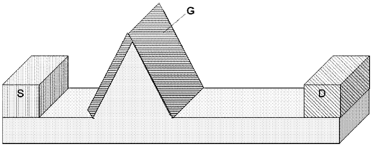
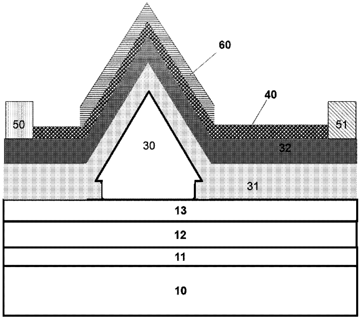
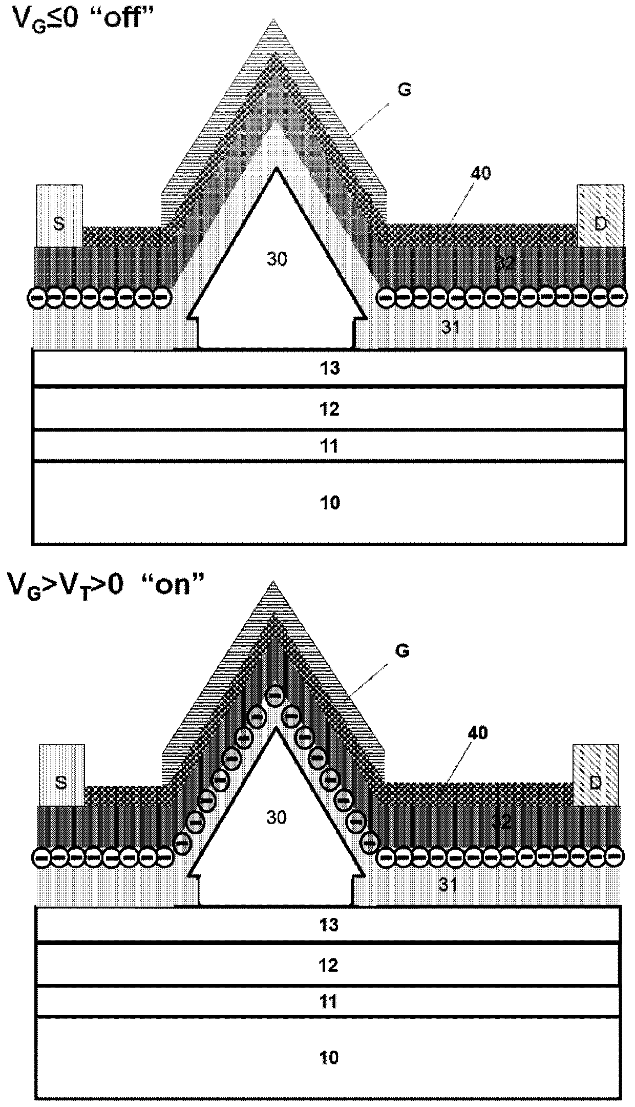
[0039] figure 1 Schematically showing a top view of a GaN-based normally-off high electron mobility transistor structure with a triangular prism slope channel provided by an embodiment of the present invention, figure 2 Schematically showing a cross-sectional view of a GaN-based normally-off high electron mobility transistor structure with a triangular prism slope channel provided by an embodiment of the present invention, as shown in figure 1 and figure 2 As shown, the GaN-based normally-off high electron mobility transistor of the triangular column slant channel may include, for example:

[0040]Substrate 10, a nucleation layer 11, a buffer layer 12, a first high-resistance GaN layer 13, a ridge-shaped GaN layer 30, a ridge-shaped channel layer 31, and a ridge barrier are sequentially formed on the surface of the substrate 10 from bottom to top. layer 32 and the ridge-shaped dielectric layer 40 , the source electrode 50 and the drain electrode 51 are prepared on the ridg...

Embodiment 2

[0052] Figure 4 Schematically showing the top view of the GaN-based normally-off high electron mobility transistor structure of the trapezoidal column slope channel provided by the embodiment of the present invention, Figure 5 A cross-sectional view schematically showing a GaN-based normally-off high electron mobility transistor structure with a trapezoidal column slope channel provided by an embodiment of the present invention, as shown in Figure 4 and Figure 5 As shown, compared with the GaN-based normally-off high electron mobility transistor of the above-mentioned triangular prism slope channel, the difference is that the structure of the slope channel is a trapezoidal column, and other structural details are the same as those of the GaN-based normal transistor of the above-mentioned triangular prism slope channel The same is true for off-type high electron mobility crystals, and will not be repeated here.

[0053] Image 6 Schematically showing the working principl...

Embodiment 3

[0056] Figure 7 Schematically shows a flow chart of a method for preparing a GaN-based normally-off high electron mobility transistor with a triangular or trapezoidal slanted channel provided by an embodiment of the present invention, as shown in Figure 7 As shown, the method may, for example, include operations S1-S5.

[0057] S1 , sequentially preparing a nucleation layer 11 , a buffer layer 12 and a first high resistance GaN layer 13 on the substrate 10 .

[0058] In a feasible manner of this embodiment, the nucleation layer 11, the buffer layer 12 and the first high-resistance GaN can be sequentially grown on the substrate 10 by Metal-organic Chemical Vapor Deposition (MOCVD). Layer 13, forming a GaN template, has a structure such as Figure 8 middle a or Figure 9 Shown in a. Wherein, the growth temperature of the nucleation layer 11 may be, for example, 500-1000°C.

[0059] S2 , preparing a patterned dielectric layer 20 on the first high resistance GaN layer 13 . ...


PUM

PropertyMeasurementUnit
thicknessaaaaaaaaaa
thicknessaaaaaaaaaa
thicknessaaaaaaaaaa

Abstract

The invention discloses a GaN-based normally-off high-electron-mobility transistor and a preparation method thereof. The method comprises the following steps of S1, sequentially preparing a nucleatinglayer (11), a buffer layer (12) and a first high-resistance GaN layer (13) on a substrate (10); S2, preparing a graphical dielectric layer (20) on the first high-resistance GaN layer (13); S3, basedon the graphical dielectric layer (20), growing a ridge-shaped GaN layer (30) in a transverse epitaxial manner, then removing the graphical dielectric layer (20), and forming a ridge-shaped GaN template, wherein the side wall of the ridge-shaped GaN layer (30) is a crystal face or a crystal face; S4, based on the ridge-shaped GaN template, growing a ridge-shaped channel layer (31) and a ridge-shaped barrier layer (32) sequentially in an epitaxial manner, wherein the thickness of the side wall of the ridge-shaped channel layer (31) and the thickness of the side wall of the ridge-shaped barrierlayer (32) are both smaller than the thickness of a platform. According to the transistor prepared by the method, etching loss and injection damage do not exist in a channel region, the influence of the etching damage on the device performance can be effectively avoided, and the GaN-based normally-off high-electron-mobility transistor has high threshold voltage, high saturation current and low on-state resistance.

Description

technical field [0001] The invention relates to the technical field of semiconductors, in particular to a GaN-based normally-off high electron mobility transistor and a preparation method thereof. Background technique [0002] Gallium nitride (GaN) material has material performance advantages such as wide band gap and high breakdown field strength, and its unique strong polarization effect can form high-density two-dimensional electron gas (2DEG). These characteristics make GaN very It is suitable for preparing power switching devices. GaN-based power switching devices have many advantages such as high power, high breakdown voltage, high frequency, high temperature resistance, radiation resistance, etc., and have good application prospects in power electronics, wireless base stations, radar, communications and other fields. [0003] Generally, the high electron mobility transistor based on the AlGaN / GaN structure is in the normally-on state due to the existence of 2DEG indu...

Claims


Application Information

Patent Timeline
Patent Type & Authority Applications(China)
IPC IPC(8): H01L21/335H01L29/778H01L29/06H01L29/10H01L29/04
CPCH01L29/045H01L29/0607H01L29/0684H01L29/0688H01L29/1029H01L29/66462H01L29/7789
Inventor 姬小利魏同波王军喜李晋闽杨富华
Owner INST OF SEMICONDUCTORS - CHINESE ACAD OF SCI
Why Eureka
Try Eureka