

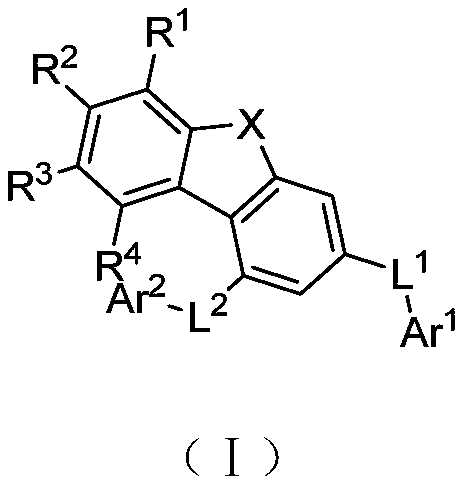
Organic light-emitting material, and organic light-emitting device
A luminescent material and organic technology, applied in luminescent materials, electrical solid devices, electrical components, etc., can solve the problems of mismatch between electrons and holes, poor luminous efficiency, poor injection effect, etc., to reduce the turn-on voltage, Good thermodynamic stability, conducive to the effect of molecular packing
- Summary
- Abstract
- Description
- Claims
- Application Information
AI Technical Summary
Problems solved by technology
Method used
Image

Examples
Embodiment 1
[0095] The glass plate coated with the ITO transparent conductive layer is ultrasonically treated in a commercial cleaning agent, rinsed in deionized water, ultrasonically degreased in acetone-ethanol mixed solvent, baked in a clean environment until the water is completely removed, and then cleaned with ultraviolet light. Light and ozone cleaning, and bombardment of the surface with a beam of low-energy cations;
[0096] Place the above-mentioned glass substrate with the anode in a vacuum chamber, and evacuate to less than 10 -5 Holder, vacuum evaporated HT-11 as the hole injection layer on the above-mentioned anode layer film, the evaporation rate is 0.1nm / s, and the evaporation film thickness is 10nm;
[0097] On the hole injection layer, HT-5 material was vacuum evaporated as the hole transport layer, the evaporation rate was 0.1nm / s, and the total film thickness was 80nm;
[0098] The light-emitting layer of the device is vacuum evaporated on the hole transport layer. Th...
Embodiment 2-6
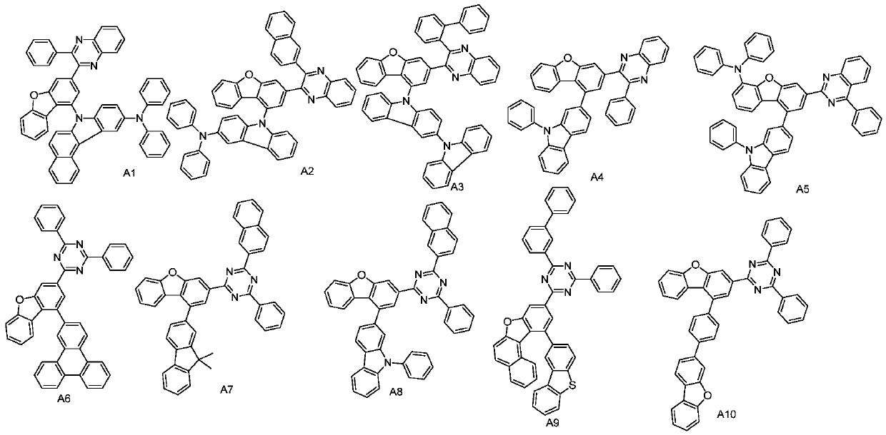
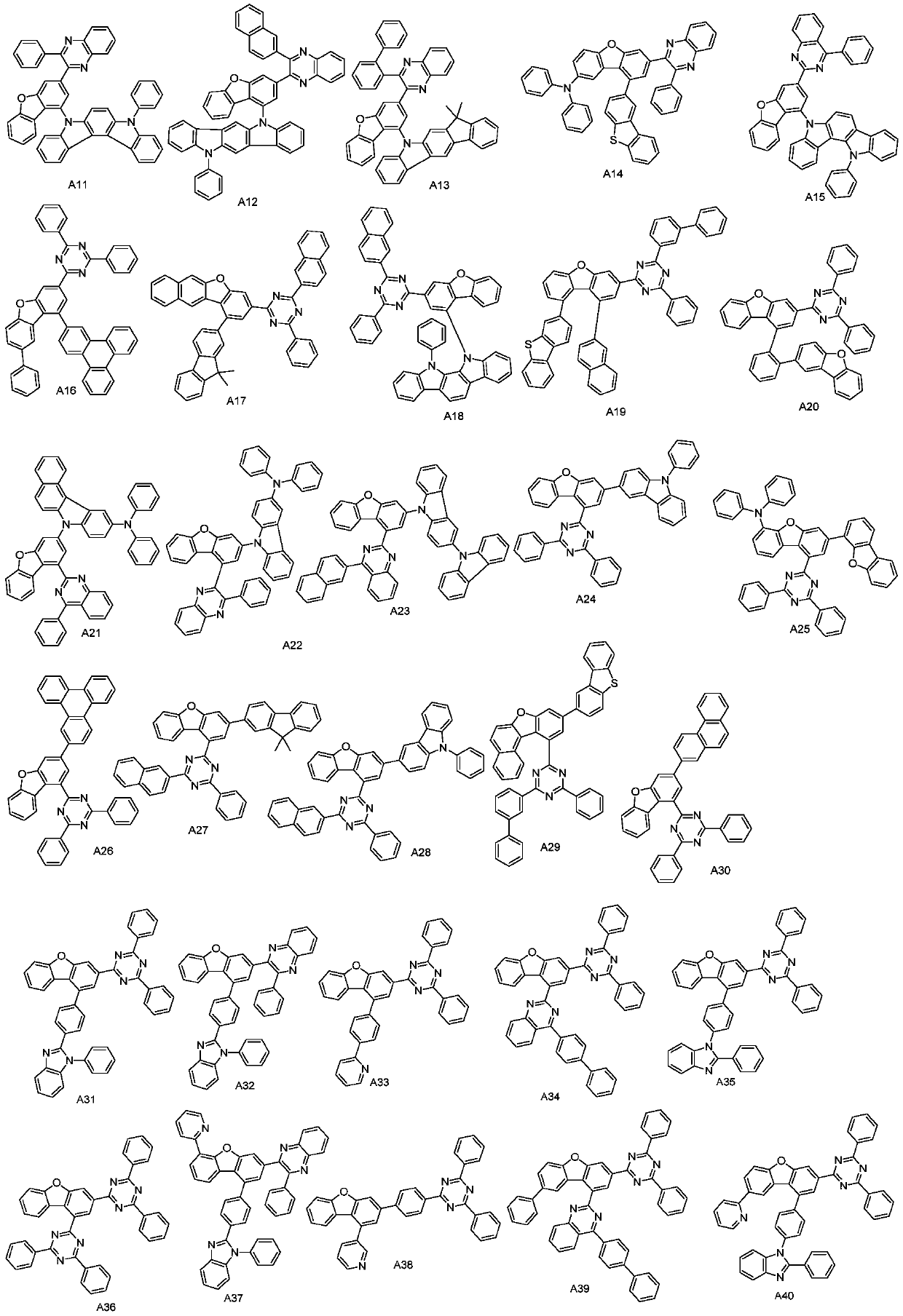
[0104] The organic light-emitting materials A6, A12, A19, A24 and A29 of the present application were respectively used as the host material of the light-emitting layer, and the rest were the same as in Example 1. The test results are shown in Table 1.
Embodiment 7
[0112] The glass plate coated with the ITO transparent conductive layer is ultrasonically treated in a commercial cleaning agent, rinsed in deionized water, ultrasonically degreased in acetone-ethanol mixed solvent, baked in a clean environment until the water is completely removed, and then cleaned with ultraviolet light. Light and ozone cleaning, and bombardment of the surface with a beam of low-energy cations;
[0113] Place the above-mentioned glass substrate with the anode in a vacuum chamber, and evacuate to less than 10 -5 , HT-11 was vacuum evaporated on the anode layer as a hole injection layer, the evaporation rate was 0.1nm / s, and the evaporation film thickness was 10nm;
[0114] On the hole injection layer, HT-5 material was vacuum evaporated as the hole transport layer, the evaporation rate was 0.1nm / s, and the total film thickness was 80nm;
[0115] The light-emitting layer of the device is vacuum-evaporated on the hole transport layer. The light-emitting layer ...
PUM
 Abstract
Description
Claims
Application Information