Stacked and spliced interdigital full-back contact perovskite solar cell and preparation method thereof

A solar cell and full back contact technology, applied in the field of solar cells, can solve problems such as limiting the utilization rate of solar cells, shading of metal electrodes, and hindering the conversion efficiency of solar cells, so as to improve the utilization rate of light, change the whole, and improve The effect of conversion efficiency

Pending Publication Date: 2020-06-19
NANKAI UNIV
View PDF9 Cites 5 Cited by
  • Summary
  • Abstract
  • Description
  • Claims
  • Application Information

AI Technical Summary

Problems solved by technology

At present, perovskite solar cells basically adopt a sandwich structure in which the electron transport layer and the hole transport layer are located on both sides of the perovskite absorption layer. Whether light is incident from the electron transport layer or from the hole transport layer, the carrier transport layer Or the transparent conductive substrate has inevitable parasitic absorption, and the metal electrode on the light-facing surface also has the problem of shading, which limits the utilization rate of solar cells to light, and thus hinders the improvement of solar cell conversion efficiency.

Method used


Image

  • Stacked and spliced interdigital full-back contact perovskite solar cell and preparation method thereof
  • Stacked and spliced interdigital full-back contact perovskite solar cell and preparation method thereof
  • Stacked and spliced interdigital full-back contact perovskite solar cell and preparation method thereof

Examples


Embodiment 1

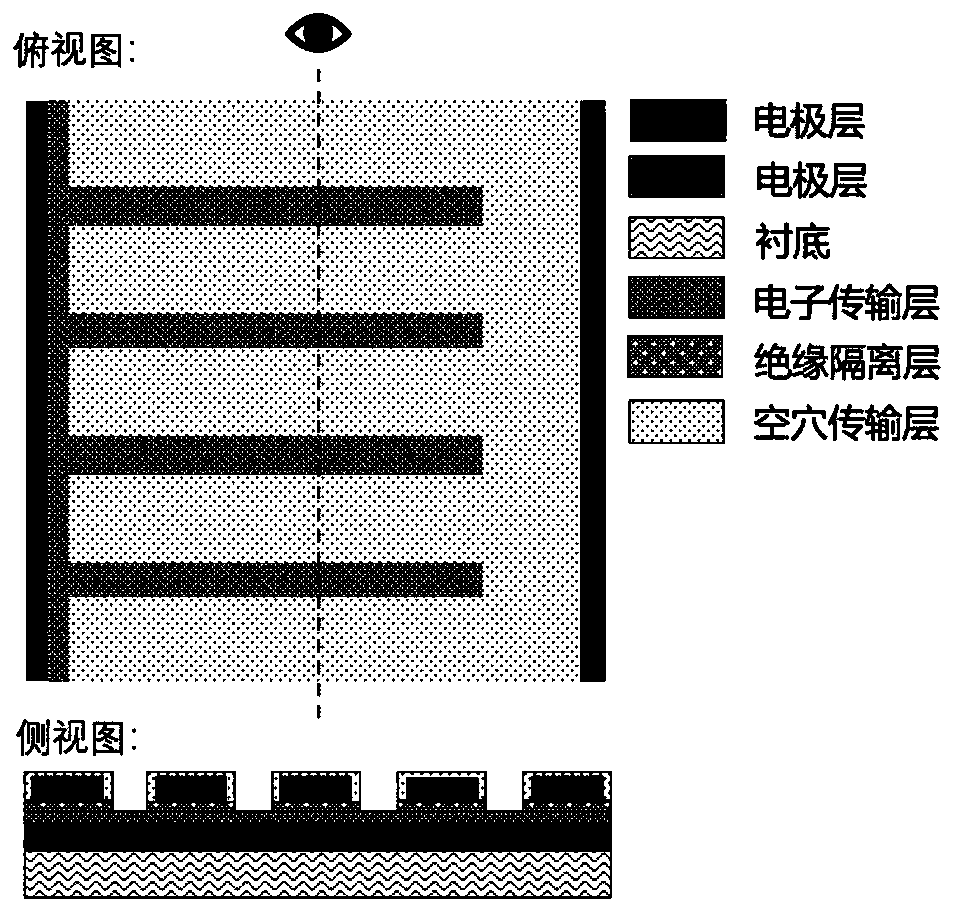
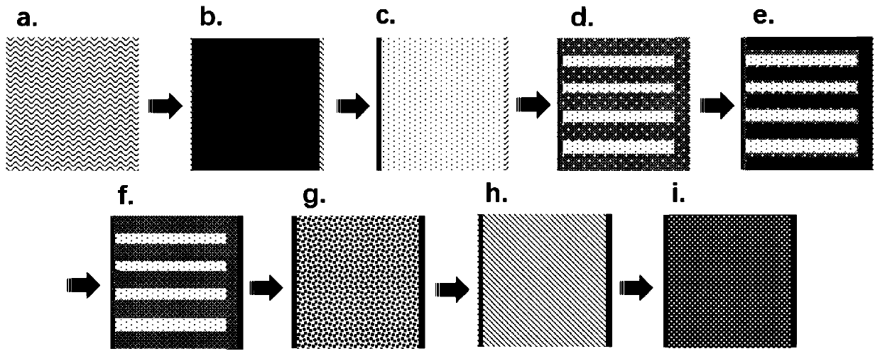
[0025] 1) Use glass as the substrate, and use ultrasonic and electronic cleaning fluid to clean it, such as image 3 a;

[0026] 2) Prepare a copper film with a thickness of 200nm by magnetron sputtering, such as image 3 b;

[0027] 3) Using evaporation deposition method and mask plate in image 3 Prepare a hole transport layer on the left comb electrode in b, such as Spiro-TPD, with a thickness of 100nm, such as image 3 c;

[0028] 4) Prepare dense SiO with a thickness of 100 nm on the hole transport layer by thermal evaporation and mask 2 film, such as image 3 d;

[0029] 5) Prepare a comb-shaped copper film with a thickness of 200nm by magnetron sputtering and a mask plate, such as image 3 e;

[0030] 6) Using thermal evaporation method and mask plate in image 3 Prepare an electron transport layer on the comb electrode in e, such as PCBM, with a thickness of 50nm, such as image 3 f;

[0031] 7) Prepare a polycrystalline perovskite absorbing layer with a thi...

Embodiment 2

[0036] 1) Use glass as the substrate, and use ultrasonic and electronic cleaning fluid to clean it, such as image 3 a;

[0037] 2) Prepare a copper film with a thickness of 100nm by thermal evaporation, such as image 3 b;

[0038] 3) Using magnetron sputtering method and mask plate in image 3 Prepare a hole transport layer on the comb electrode in b, such as NiO x , thickness 100nm, such as image 3 c;

[0039] 4) Prepare dense SiO with a thickness of 100 nm on the hole transport layer by magnetron sputtering and mask 2 film, such as image 3 d;

[0040] 5) Prepare a comb-shaped titanium film with a thickness of 100nm by thermal evaporation method and mask plate, such as image 3 e;

[0041] 6) Using magnetron sputtering method and mask plate in image 3 Preparation of electron transport layer on the comb electrode in e, such as TiO 2 , thickness 50nm, such as image 3 f;

[0042] 7) Prepare a polycrystalline perovskite absorbing layer with a thickness of 500 n...

Embodiment 3

[0047] 1) Use glass as the substrate, and use ultrasonic and electronic cleaning fluid to clean it, such as image 3 a;

[0048] 2) A gold film with a thickness of 50nm was prepared by magnetron sputtering, such as image 3 b;

[0049] 3) Prepare dense Al with a thickness of 20 nm on the hole transport layer by chemical vapor deposition and mask 2 o 3 film, such as image 3 d;

[0050] 4) Prepare a comb-shaped titanium film with a thickness of 100nm by thermal evaporation and a mask, such as image 3 e;

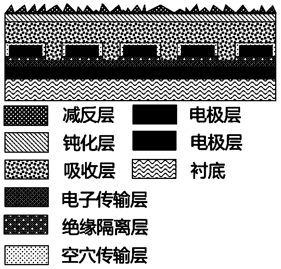
[0051] 5) Prepare a polycrystalline perovskite absorbing layer with a thickness of 700nm by one-step solution spin coating method, such as image 3 g;

[0052] 6) Prepare a KI passivation layer with a thickness of 15nm by thermal evaporation, such as image 3 h;

[0053] 7) Preparation of SiO with low refractive index by electron beam evaporation 2 / MgF 2 Dense anti-reflection protective layer with a thickness of 100nm, such as image 3 i.

[0054] 8) Prepared w...


PUM

PropertyMeasurementUnit
thicknessaaaaaaaaaa
thicknessaaaaaaaaaa
widthaaaaaaaaaa

Abstract

The invention discloses a stacked and spliced interdigital full-back contact perovskite solar cell. The cell sequentially comprises the following components from bottom to top: 1) a substrate; 2) a positive electrode; 3) a hole transport layer on the positive electrode; 4) an insulating isolation layer; 5) a negative electrode; 6) an electron transport layer on the negative electrode; 7) a perovskite absorption layer; 8) a passivation layer; and 9) an antire-flection protective layer. The solar cell is characterized in that the positive electrode and the negative electrode are arranged on thebacklight surface of the cell in an up-and-down overlapping manner, an upper electrode does not completely cover a lower electrode, and the positive electrode and the negative electrode are separatedfrom each other through insulating material filling and the like. The passivation layer can reduce surface defects and carrier recombination caused by the surface defects; and the anti-reflection protective layer plays a role in reducing light loss and protecting the perovskite layer at the same time. The stacked and spliced interdigital full-back-contact perovskite solar cell disclosed by the invention can completely avoid the shading loss of the front electrode and the parasitic absorption of a carrier transport layer or the transparent conductive substrate, and improve the light utilizationefficiency and photoelectric conversion efficiency of the perovskite solar cell.

Description

technical field [0001] The invention relates to a solar cell, in particular to a stacked interdigitated full-back contact perovskite solar cell. [0002] technical background [0003] The depletion of fossil energy is posing a major threat to the sustainable development of human society. Solar energy is a renewable and clean energy source. Therefore, solar cells are valued for their safety and reliability, no noise, no pollution emissions, no risk of depletion, and no geographical restrictions on resource distribution. [0004] At present, the leading product in the photovoltaic market is crystalline silicon solar cells, but there is less and less room for its efficiency improvement and cost reduction. Therefore, the development of new photovoltaic materials and devices has attracted the attention of various countries. In 2009, the efficiency of the first solar cell based on organic / inorganic metal halide perovskite materials was only 3.8%, but its efficiency has reached 25...

Claims


Application Information

Patent Timeline
Patent Type & Authority Applications(China)
IPC IPC(8): H01L51/42H01L51/44H01L51/46H01L51/48
CPCH10K85/30H10K30/81H10K30/00H10K30/82H10K30/88Y02E10/549
Inventor 李跃龙侯国付赵颖张晓丹
Owner NANKAI UNIV
Why Eureka
Try Eureka