LED chip capable of improving external quantum efficiency, and preparation method thereof

An LED chip and external quantum efficiency technology are applied in the field of LED chips and their preparation for improving external quantum efficiency, so as to achieve the effects of improving external quantum efficiency, improving luminous efficiency and simple process operation.

Pending Publication Date: 2020-07-28
XIANGNENG HUALEI OPTOELECTRONICS
View PDF0 Cites 0 Cited by
  • Summary
  • Abstract
  • Description
  • Claims
  • Application Information

AI Technical Summary

Problems solved by technology

[0006] The purpose of the present invention is to provide an LED chip with improved external quantum efficiency and its preparation method to solve the problem of improving the reflectivity of the reflective electrode while ensuring the adhesion between the electrode and the transparent conductive layer

Method used


Image

  • LED chip capable of improving external quantum efficiency, and preparation method thereof
  • LED chip capable of improving external quantum efficiency, and preparation method thereof
  • LED chip capable of improving external quantum efficiency, and preparation method thereof

Examples


Embodiment 1

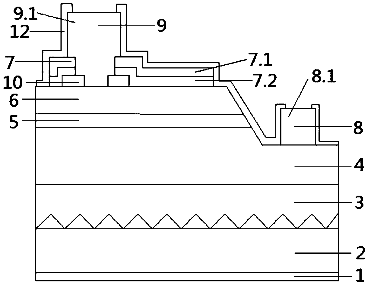
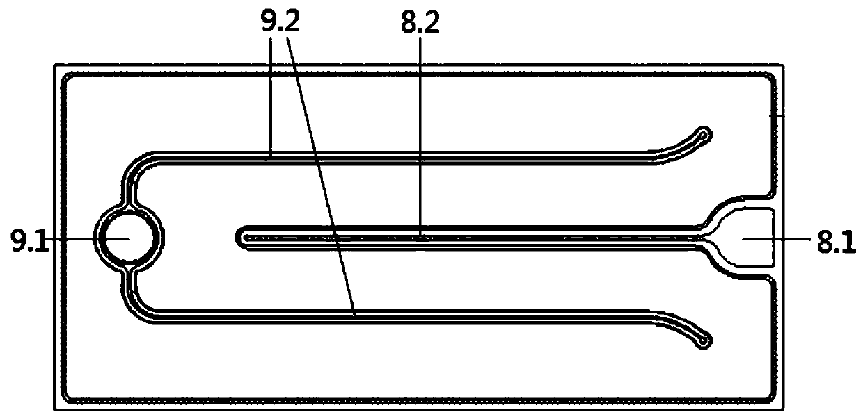
[0053] See Figure 1 to Figure 11 , An LED chip with improved external quantum efficiency and a preparation method thereof, this embodiment is applied to improve the external quantum efficiency of the LED chip.

[0054] An LED chip with improved external quantum efficiency, see figure 1 , Including from bottom to top:

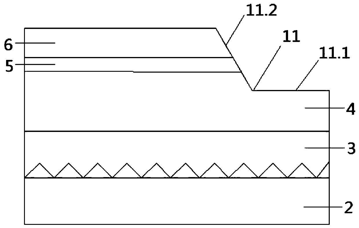
[0055] DBR layer 1. In this embodiment, the DBR material is silicon dioxide (SiO 2 ) And titanium dioxide (TiO 2 ) Alternate structure, the refractive indices of the two materials are between 1.45~1.52 and 2.45~2.55, and the thickness of each layer is determined by optical software simulation to form a distributed Bragg reflector (DBR) whose reflectivity is in the visible wavelength range ( 380~800nm) greater than 95%;

[0056] The substrate 2 located on the DBR layer 1. In this embodiment, the substrate 2 is a sapphire substrate (PSS substrate);

[0057] A buffer layer 3 on the substrate 2;

[0058] The first semiconductor layer 4 located on the buffer layer 3. In thi...

Embodiment 2

[0086] The difference between Example 2 and Example 1 is that the selected electron beam evaporation zinc oxide deposition temperature is 250°C, and the others are the same as Example 1. Under this combination of process parameters, the obtained AZO layer 7.1 has uniform crystal grains and crystal grain size Between 30nm and 50nm, the thrust experiment meets the requirements, and the brightness of the LED chip is improved.

Embodiment 3

[0088] The difference between Example 3 and Example 1 is that the selected electron beam evaporation zinc oxide deposition temperature is 300°C, and the rotation speed of the plating pot is 60r / min. Others are the same as Example 1. Under this combination of process parameters, the AZO layer obtained 7.1 The crystal grain is uniform, and the crystal grain size is between 30nm and 50nm. After the electrode is plated, the pad shows a slight black spot, which affects the appearance, but does not affect the bonding wire. The thrust experiment meets the requirements, and the brightness of the LED chip is improved.


PUM

PropertyMeasurementUnit
particle sizeaaaaaaaaaa
thicknessaaaaaaaaaa
thicknessaaaaaaaaaa

Abstract

The invention provides an LED chip capable of improving external quantum efficiency. The LED chip comprises a DBR layer, a substrate, a buffer layer, a first semiconductor layer, an active layer, a second semiconductor layer, a transparent conductive layer, an N type electrode and a P type electrode, wherein the N type electrode and the P type electrode are both aluminum-based reflection electrodes, and the aluminum metal layer of the P type electrode is in direct contact with the transparent conductive layer to improve the reflectivity of a reflection electrode and a semiconductor interface.The invention further provides a preparation method of the LED chip capable of improving the external quantum efficiency. The method comprises the following steps: growing a complete LED structure epitaxial wafer on a substrate, and etching to form a semiconductor structure with a step inclined plane; manufacturing a current blocking layer and a transparent conductive layer comprising an AZO layer; preparing a P type electrode, an N type electrode and a passivation layer, and performing back plating of a DBR layer; and preparing the wafer into the LED chip device. According to the invention, the aluminum-based reflecting electrode is adopted, and the insertion layer metal between the P type electrode and the transparent conductive layer is canceled, so that the luminous efficiency of the LED chip is improved, and the external quantum efficiency of the LED chip is improved.

Description

Technical field [0001] The invention relates to the technical field of LED chip manufacturing, in particular to an LED chip with improved external quantum efficiency and a preparation method thereof. Background technique [0002] Since the breakthrough of p-gallium nitride (p-GaN) in 1992, GaN-based light-emitting diode (LED) technology has made rapid progress. The internal quantum efficiency of the LED chip has been greatly improved, reaching over 80%, but the external quantum efficiency is still very low. [0003] In order to improve the external quantum efficiency of LEDs, many process technologies have been developed. One of them is the use of reflective electrodes. The principle of reflective electrode technology is that the electrode metal is opaque in the visible light range, while traditional LED chips have two electrodes mounted on the same side. , Are all on the light-emitting surface of the LED chip, so the electrode metal blocks the light emitted from the active area, ...

Claims


Application Information

Patent Timeline
Patent Type & Authority Applications(China)
IPC IPC(8): H01L33/14H01L33/38H01L33/40H01L33/46H01L33/00C23C14/08C23C14/18C23C14/24C23C14/30C23C14/35C23C14/54C23C14/58C23C16/02C23C16/34C23C16/40C23C16/50C23C16/56
CPCC23C14/086C23C14/18C23C14/24C23C14/30C23C14/35C23C14/54C23C14/5806C23C14/5873C23C16/0245C23C16/34C23C16/402C23C16/407C23C16/50C23C16/56H01L33/0075H01L33/145H01L33/385H01L33/405H01L33/46
Inventor 汪延明周智斌
Owner XIANGNENG HUALEI OPTOELECTRONICS
Why Eureka
Try Eureka