Method for selectively metallizing oxide ceramic composite material

A technology of oxide ceramics and composite materials, applied in metal processing equipment, laser welding equipment, electrical components, etc., can solve the problems of weak interface bonding force, poor wettability between oxide ceramic materials and metal materials, etc. The effect of strong binding force and controllable process

Pending Publication Date: 2020-08-11
苏州赋金科技有限公司
View PDF9 Cites 0 Cited by
  • Summary
  • Abstract
  • Description
  • Claims
  • Application Information

AI Technical Summary

Problems solved by technology

However, the key factor restricting its application is the poor wettability between oxide ceramic materials and metal materials, and the interface bonding force is not strong.

Method used


Image

  • Method for selectively metallizing oxide ceramic composite material
  • Method for selectively metallizing oxide ceramic composite material
  • Method for selectively metallizing oxide ceramic composite material

Examples


Embodiment 1

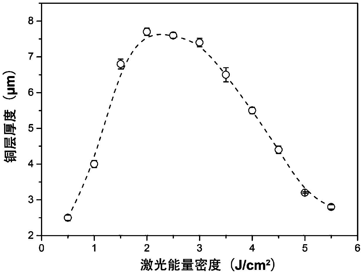
[0022] al 2 o 3 -Cu 2 Copper clad metallization of O composite materials: Al 2 o 3 and Cu 2 O batching according to mass ratio 96:4, dry mixing with agate ball grinding medium for 2 hours to obtain uniformly mixed powder, then put the powder into a steel mill of 50mm×50mm for cold pressing, the pressure is 50MPa, and then The green body is sintered in a vacuum furnace, and the furnace temperature is raised to 1630°C at a heating rate of 5°C / min, and the holding time is 4 hours to obtain Al 2 o 3 -Cu 2 O composite material, then use laser for surface treatment and wiring, laser energy density: 0.6-20j / cm 2 , and then use the standard copper plating solution (Yishun brand Q / YS.118) for copper sinking treatment. The relationship between the thickness of copper sinking and laser energy density is as follows: figure 2 shown.

Embodiment 2

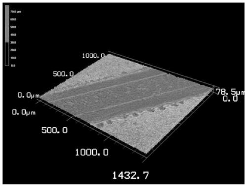
[0024] Copper clad metallization of 3YSZ-CuO composite materials: ZrO 2 -3%Y 2 o 3 (3YSZ) and CuO are mixed according to the mass ratio of 98:2, with agate balls and absolute alcohol as the grinding medium, mixed in a ball mill for 2 hours and then dried to obtain a uniformly mixed powder material, and then the powder is put into a 50mm Cold pressing was carried out in a steel abrasive tool of ×50mm at a pressure of 100MPa, and then the green body was sintered in a vacuum furnace, and the furnace temperature was raised to 1430°C at a heating rate of 5°C / min, and the holding time was 2 hours to obtain 3YSZ-CuO Composite material, remaining steps are identical with embodiment 1, carry out surface treatment and the surface of wiring with laser such as image 3 shown.

Embodiment 3

[0026] al 2 o 3 -NiO composite nickel clad metallization: the Al 2 o 3 Mix with NiO according to the mass ratio of 95:5, and dry mix with agate ball grinding medium for 1 hour to obtain a uniformly mixed powder, and then put the powder into a 50mm×50mm steel grinding tool for cold pressing at a pressure of 80MPa. Then the green body is sintered in a vacuum furnace, and the furnace temperature is raised to 1650°C at a heating rate of 5°C / min, and the holding time is 4 hours to obtain Al 2 o 3 -NiO composite material, then use laser for surface treatment and wiring, and then use standard nickel deposition solution (Yishun brand Q / YS.602) for nickel deposition treatment.

Description of drawings

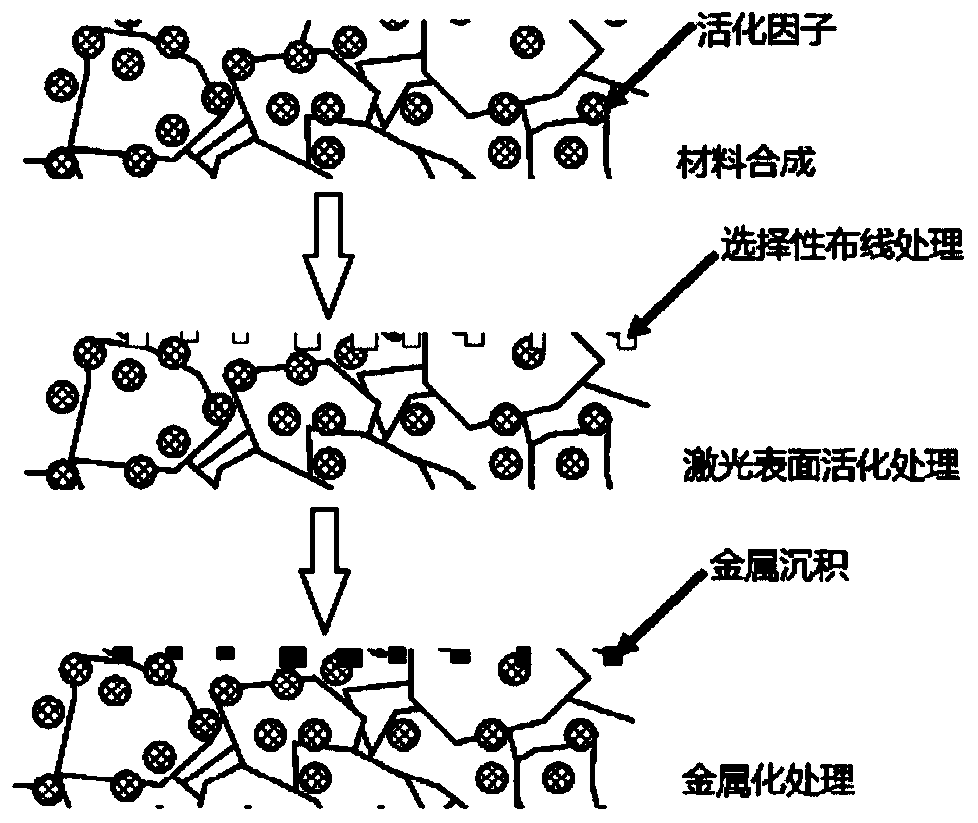
[0027] figure 1 : Schematic diagram of laser surface treatment and post-wiring metallization after adding activating factors in oxide ceramic materials.

[0028] figure 2 :Al 2 o 3 -Cu 2 The relationship between the thickness of deposited copper and the laser energy density ...


PUM


Abstract

The invention relates to a technology for selectively metallizing the surface of an oxide ceramic composite material by using a laser surface treatment technology. According to the specific scheme, the technology comprises the following steps: 1) preparing an oxide ceramic composite material containing active factors; and 2) activating the surface of the oxide ceramic and ablating the circuit by using laser according to the circuit drawing; 3) cleaning the ablated sample, putting the ablated sample into a chemical liquid for metallization treatment, and depositing a metal circuit; and 4) drying the cleaned sample. Compared with a traditional metallization process, the method has the advantages of being simpler, faster in preparation, more controllable in process, high in precision, high inbinding force, more environmentally friendly and the like. According to the characteristics of coated metal, the coating has the properties of heat conduction, electric conduction, magnetic conduction and the like, and has very high application value in the fields of large-scale integrated circuits, electromagnetic shielding, multifunctional chips and the like.

Description

technical field [0001] A method for selective metallization on the surface of an oxide ceramic composite material by using laser surface treatment technology. Background technique [0002] With the development of electronic technology and semiconductors, the integration of chips continues to increase, the width of circuit wiring becomes finer, and the power dissipation per unit area is getting larger and larger, which will inevitably cause an increase in heat generation and easily cause device failure. Therefore, in recent years, ceramic PCB substrate circuit printing technology has attracted more and more attention. Ceramic PCB circuit substrate refers to a special process board that directly bonds functional metal materials to the surface of a ceramic substrate (single-sided or double-sided) under certain conditions. The made ultra-thin composite substrate has excellent electrical insulation properties, high thermal conductivity, excellent solderability and high adhesion ...

Claims


Application Information

Patent Timeline
IPC IPC(8): C04B35/10C04B35/48C04B35/14C04B35/46C04B35/622C04B41/88C04B41/91B23K26/362H05K3/18
CPCB23K26/362C04B35/10C04B35/14C04B35/46C04B35/48C04B35/622C04B41/5127C04B41/5144C04B41/5346C04B41/88C04B41/91C04B2235/3225C04B2235/3279C04B2235/3281C04B2235/6562C04B2235/6567H05K3/181C04B41/455C04B41/4535
Inventor 贝国平
Owner 苏州赋金科技有限公司
Why Eureka
Try Eureka