

Preparation method of 1550 nm waveband single photon source, single photon source and optical device
A single photon source and optical device technology, applied in semiconductor devices, electrical components, circuits, etc., can solve the problems of difficulty in preparing 1550nm light source, large deviation of film thickness, crystal quality cannot reach single crystal, etc., and achieve the effect of overcoming preparation difficulties
- Summary
- Abstract
- Description
- Claims
- Application Information
AI Technical Summary
Problems solved by technology
Method used
Image

Examples
Embodiment 1
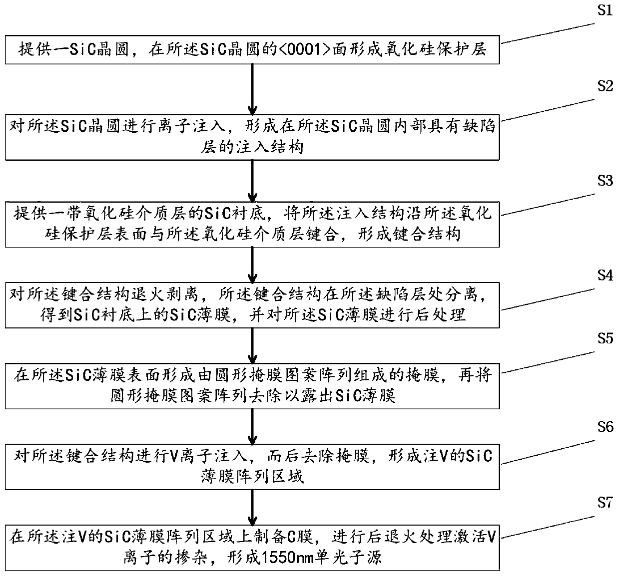
[0042] This embodiment provides a method for preparing a 1550nm band single photon source. The preparation method in this embodiment at least includes the following steps:
[0043] S1. Provide a SiC wafer 1, and form a silicon oxide protective layer 2 on the surface of the SiC wafer 1 by wet thermal oxidation. The thermal oxidation temperature is 1000°C, the oxidation time is 24h, and the thickness of the silicon oxide protective layer 2 is 5 μm;
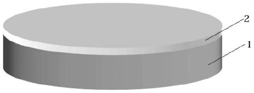
[0044] S2. Implanting ions along the surface to perform H ion implantation on the SiC wafer 1 to form an implanted structure with a defect layer 3 inside the SiC wafer 1, and the implantation dose is 1×10 18 cm -2 , the injection energy is 2MeV;
[0045] S3. Provide a polycrystalline SiC substrate 4 with a silicon oxide dielectric layer 5, and bond the implanted structure to the silicon oxide dielectric layer 5 along the surface of the silicon oxide protective layer 2 to form a bonding structure 6, wherein the thickness of the S...
Embodiment 2
[0052] This embodiment provides a method for preparing a 1550nm band single photon source. The preparation method in this embodiment at least includes the following steps:
[0053] S1. Provide a SiC wafer 1, and form a silicon oxide protective layer 2 on the surface of the SiC wafer 1 by wet thermal oxidation. The thermal oxidation temperature is 1000°C, the oxidation time is 2h, and the thickness of the silicon oxide protective layer 2 is 3 μm;
[0054] S2. Implanting ions along the surface to perform H ion implantation on the SiC wafer 1 to form an implanted structure with a defect layer 3 inside the SiC wafer 1, and the implantation dose is 1×10 17 cm -2 , the injection energy is 1.5MeV;
[0055] S3. Provide a polycrystalline SiC substrate 4 with a silicon oxide dielectric layer 5, and bond the implanted structure to the silicon oxide dielectric layer 5 along the surface of the silicon oxide protective layer 2 to form a bonding structure 6, wherein the thickness of the ...
Embodiment 3
[0061] This embodiment provides a method for preparing a 1550nm band single photon source. The preparation method in this embodiment at least includes the following steps:
[0062] S1. Provide a SiC wafer 1, and form a silicon oxide protective layer 2 on the surface of the SiC wafer 1 by wet thermal oxidation. The thermal oxidation temperature is 1150°C, the oxidation time is 10 minutes, and the thickness of the silicon oxide protective layer 2 is 200nm;
[0063] S2. Implanting ions along to perform He ion implantation on the SiC wafer 1 to form an implanted structure with a defect layer 3 inside the SiC wafer 1, and the implantation dose is 1×10 17 cm -2 , the injection energy is 1MeV;
[0064] S3. Provide an α-SiC substrate 4 with a silicon oxide dielectric layer 5, and bond the implanted structure to the silicon oxide dielectric layer 5 along the surface of the silicon oxide protection layer 2 to form a bonding structure 6, wherein the thickness of the SiC substrate 4 i...
PUM
| Property | Measurement | Unit |
|---|---|---|
| Thickness | aaaaa | aaaaa |
| Thickness | aaaaa | aaaaa |
| Thickness | aaaaa | aaaaa |
Abstract
Description
Claims
Application Information