Surface-enhanced Raman scattering substrate and preparation method and application thereof
A surface-enhanced Raman and substrate technology, applied in the direction of Raman scattering, measuring devices, instruments, etc., can solve the problems of poor manufacturability, sensitivity, poor uniformity and stability, inconvenient portability, etc., and achieve the effect of high Raman enhanced performance
- Summary
- Abstract
- Description
- Claims
- Application Information
AI Technical Summary
Problems solved by technology
Method used
Image
Examples
preparation example Construction
[0034] The present invention also provides a method for preparing the surface-enhanced Raman scattering substrate, comprising the following steps:
[0035] (1) Use a laser to scan the base material in point form to form a three-dimensional self-supporting micro-nano composite multilevel structure; the laser is a femtosecond laser or a picosecond laser; the base material is a transition metal;
[0036] (2) Washing, purging, and drying the obtained three-dimensional self-supporting micro-nano composite multi-level structure in sequence to obtain the surface-enhanced Raman scattering substrate.
[0037] In the present invention, the base material is preferably processed before spot scanning, and the processing is preferably sequential grinding, cleaning and purging, and the grinding is preferably performed with sandpaper, and the mesh number of the sandpaper is It is preferably 200 mesh, 500 mesh, 1000 mesh and 1200 mesh. The order of grinding is preferably from low mesh to high ...
Embodiment 1
[0048] A surface-enhanced Raman scattering substrate and its preparation method
[0049] Pre-treatment: Cut the copper block, the size is 10×10×2.5mm 3 , using 200-mesh, 500-mesh, 1000-mesh and 1200-mesh sandpaper to polish sequentially. The grinding time of each kind of sandpaper is 1 minute. The polished copper block is soaked in ethanol for 5 minutes and the ultrasonic frequency is 53KHz. After the ultrasonic is finished, Nitrogen was purged at a pressure of 0.1 MPa for 5 min to obtain a dry copper substrate.
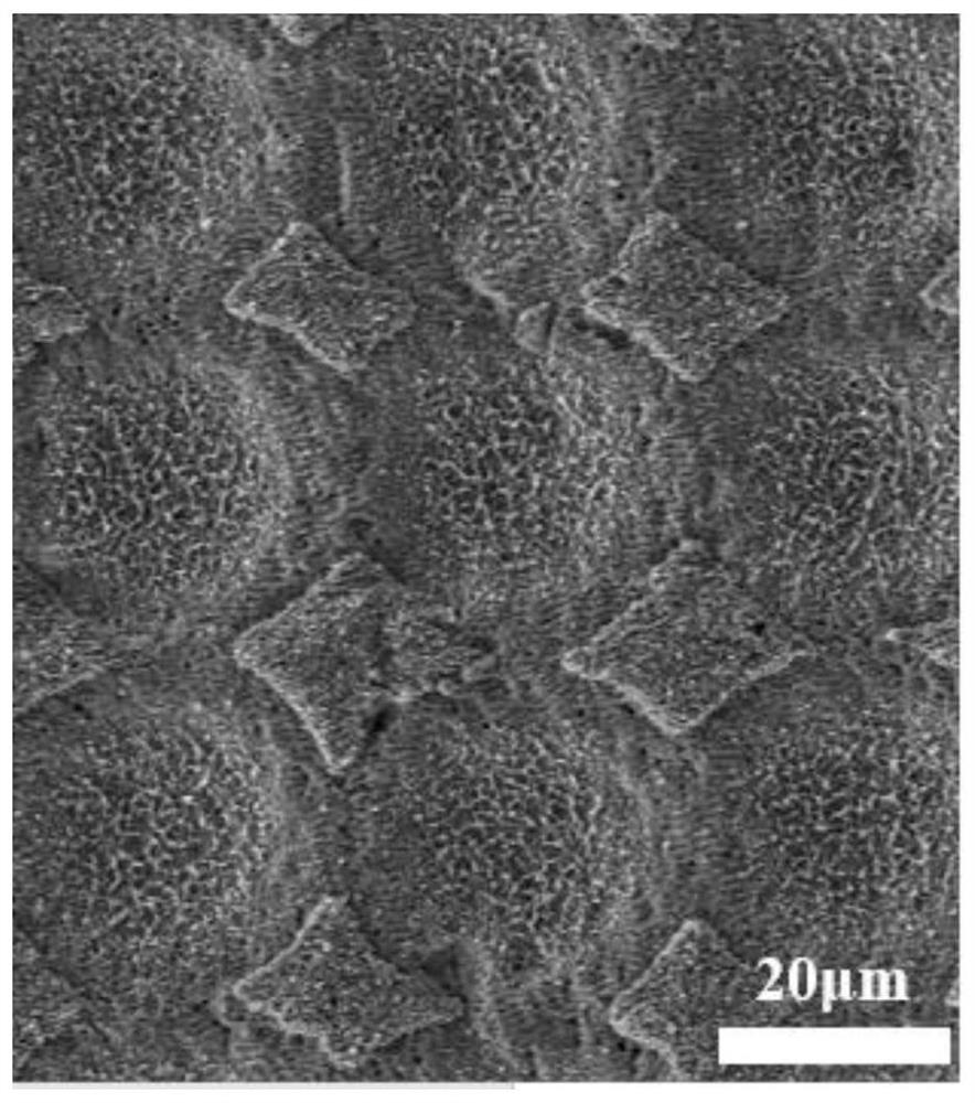
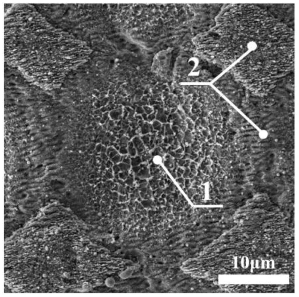
[0050] A femtosecond laser is used to ablate the surface of the copper substrate. The laser wavelength is 1030nm, the pulse width is 800fs, the pulse repetition frequency is 200kHz, the average power is 10W, and the scan time is 30s, and the scan interval is 50μm. , to get the intermediate sample;
[0051] After washing the intermediate sample with ethanol, purging with nitrogen, the purging pressure is 0.1 MPa, and the purging time is 5 minutes. After purging, it ...
Embodiment 2
[0060] A surface-enhanced Raman scattering substrate and its preparation method
[0061] Cut the silver sheet to size 10×10×0.1mm 3 small pieces of matrix;
[0062] A femtosecond laser is used to ablate the surface of the silver substrate, wherein the laser wavelength is 532nm, the pulse width is 300fs, the pulse repetition frequency is 600kHz, the average power is 20W, and the scanning time is 30s, and the scanning interval is 50μm. , to get the intermediate sample;
[0063] After washing the intermediate sample with ethanol, purging with nitrogen, the purging pressure is 0.1 MPa, and the purging time is 5 minutes. After purging, it is dried at 100° C. for 15 minutes to obtain a silver surface-enhanced Raman scattering substrate.
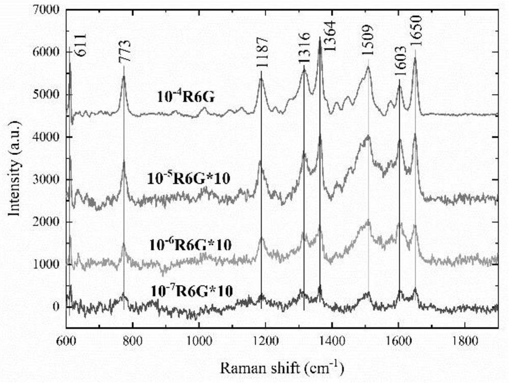
[0064] The surface-enhanced Raman scattering substrate prepared in this application has a micro-pit array period of 50 μm and a micro-pit depth of 10 μm. The surface scanning picture is shown in Figure 7; the substrate prepared in this example ha...
PUM
| Property | Measurement | Unit |
|---|---|---|
| depth | aaaaa | aaaaa |
| diameter | aaaaa | aaaaa |
| wavelength | aaaaa | aaaaa |
Abstract
Description
Claims
Application Information
 - R&D
- Intellectual Property
- Life Sciences
- Materials
- Tech Scout
- Unparalleled Data Quality
- Higher Quality Content
- 60% Fewer Hallucinations
Browse by: Latest US Patents, China's latest patents, Technical Efficacy Thesaurus, Application Domain, Technology Topic, Popular Technical Reports.
© 2025 PatSnap. All rights reserved.Legal|Privacy policy|Modern Slavery Act Transparency Statement|Sitemap|About US| Contact US: help@patsnap.com


