Trench silicon carbide power device with low on-resistance and manufacturing process thereof

A low on-resistance, power device technology, applied in the field of silicon carbide trench MOS devices and their manufacturing processes, can solve the problems of complex process flow, high interface state density, device failure gate leakage, etc. Process difficulty and effect on equipment requirements

Active Publication Date: 2020-09-15
SOUTHEAST UNIV
View PDF0 Cites 7 Cited by
  • Summary
  • Abstract
  • Description
  • Claims
  • Application Information

AI Technical Summary

Problems solved by technology

However, today's trench-type silicon carbide devices still have shortcomings, such as the corners of trench-type devices are prone to breakdown, so a P-type shielding layer is usually introduced under the trench to optimize the electric field distribution at the corners, which can effectively improve the reliability of the device. But this also introduces additional JFET area, which increases the on-resistance of the device
To this end, the researchers proposed an N-type buried layer all-encapsulated P shielding layer structure, which effectively reduces the width of the JFET region and reduces the on-resistance; however, this structure introduces the peak value of the electric field into the sharp corner of the trench. , will cause the oxide layer to degr

Method used


Image

  • Trench silicon carbide power device with low on-resistance and manufacturing process thereof
  • Trench silicon carbide power device with low on-resistance and manufacturing process thereof
  • Trench silicon carbide power device with low on-resistance and manufacturing process thereof

Examples


Embodiment 1

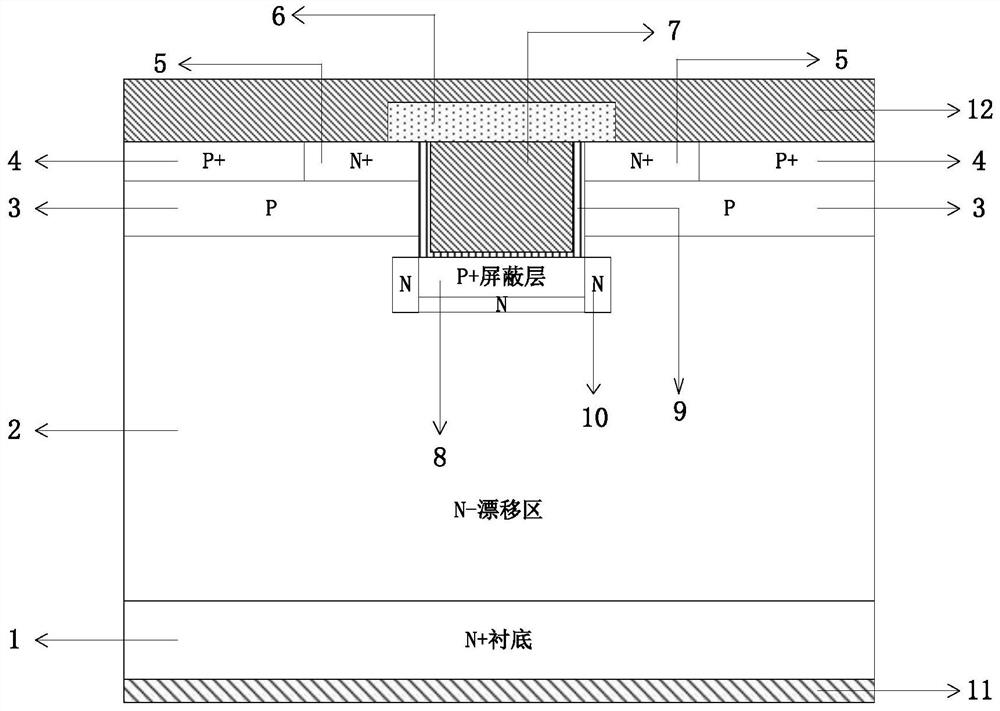
[0034]A trench silicon carbide power device with low on-resistance, comprising: an N-type substrate 1, a drain metal 11 is provided on one side of the N-type substrate 1, and a drain metal 11 is provided on the other side of the N-type substrate 1. The N-type epitaxial layer 2 is provided with a P-type body region 3 on the N-type epitaxial layer 2, and an N-type source region 5 and a P-type body contact region 4 are arranged on the P-type body region 3, and the P-type body contact region 4 is located outside the N-type source region 5, and a trench is opened on the N-type source region 5. The trench passes through the N-type source region 5 and the P-type body contact region 4 and enters the N-type epitaxial layer 2. A gate oxide layer 9 is provided on the bottom and inner walls, a polysilicon gate 7 is provided in the gate oxide layer 9, a passivation layer 6 is covered on the top of the trench, a P-type shielding layer 8 is provided under the trench, and a P-type shielding la...

Embodiment 2

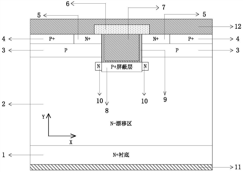
[0037] A manufacturing process of trench silicon carbide power devices with low on-resistance, with figure 2 The XY axis shown is the reference, including the following steps:

[0038] Take an N-type substrate 1, and make an N-type epitaxial layer 2 on one surface of the N-type substrate 1. The N-type epitaxial layer 2 is made by epitaxially growing a part of the N-type epitaxial layer on the N-type substrate 1. On the grown N-type epitaxial layer, ion implantation is used to form a P-type shielding layer 8 and an N-type buried layer 10, and then another part of the N-type epitaxial layer is epitaxially grown, and the two parts of the N-type epitaxial layer are stacked to form a complete N-type epitaxial layer. type epitaxial layer 2;

[0039] Prepare the P-type body region 3, the N-type source region 5, and the P-type body contact region 4 on the other N-type epitaxial layer according to this, and then perform groove etching on the N-type source region 5, and the groove As...


PUM


Abstract

The invention provides a trench silicon carbide power device with low on-resistance and a manufacturing process thereof. The cell of the trench silicon carbide power device comprises an N-type substrate, an N-type epitaxial layer and a trench, wherein the trench is internally provided with a gate oxide layer and a polysilicon gate, a P-type body region, an N-type source region and a P+ body contact region are arranged on the two sides of the trench, a P shielding layer is arranged below the trench, and an N-type buried layer is arranged on the side of the P shielding layer. The manufacturing process of the N-type buried layer comprises the steps of epitaxially growing a first part of an N-type drift region on the N-type substrate, forming a P shielding layer and an N-type buried layer on the first part of the N-type drift region by adopting an ion implantation process, continuing to epitaxially form a second part of the N-type drift region, and carrying out a subsequent process flow. According to the invention, two sides of the P shielding layer are provided with the N-type buried layers, the electric field peak is moved downwards, the trench corner electric field is reduced, the interface state density and defects are reduced, and the reliability of the gate oxide layer is improved; and an N-type buried layer below is eliminated, the gate charge of the device is reduced, the switching characteristic is improved, and the withstand voltage of the device is further improved.

Description

technical field [0001] The invention belongs to the technical field of power semiconductors, and in particular relates to a silicon carbide trench MOS device and a manufacturing process thereof. Background technique [0002] The third-generation wide-bandgap semiconductor material SiC has the advantages of high saturation drift speed and high thermal conductivity. It is widely used in the field of power semiconductors and has good development prospects. Compared with Si-type MOSFETs, MOSFETs made of SiC materials effectively reduce the device volume. , improved integration. Compared with the planar gate MOS device, the trench type MOS device eliminates the JFET region, increases the channel density and reduces the on-resistance of the device. However, today's trench-type silicon carbide devices still have shortcomings, such as the corners of trench-type devices are prone to breakdown, so a P-type shielding layer is usually introduced under the trench to optimize the electri...

Claims


Application Information

Patent Timeline
IPC IPC(8): H01L29/78H01L29/06H01L21/04
CPCH01L29/7813H01L29/0623H01L21/046H01L29/66068Y02B70/10
Inventor 魏家行周华付浩隗兆祥严晓雯刘斯扬孙伟锋时龙兴
Owner SOUTHEAST UNIV
Why Eureka
Try Eureka