Solar cell and preparation method thereof

A solar cell and electrode technology, applied in circuits, photovoltaic power generation, electrical components, etc., can solve problems such as damage to the borosilicate glass layer and overetching of silicon wafers

Pending Publication Date: 2020-09-15
ZHEJIANG JINKO SOLAR CO LTD +1
View PDF3 Cites 12 Cited by
  • Summary
  • Abstract
  • Description
  • Claims
  • Application Information

AI Technical Summary

Problems solved by technology

In the process of doping amorphous silicon on the back side with phosphorus, phosphorus will also diffuse to the front side of the silicon wafer, destroying the borosilicate gla

Method used


Image

  • Solar cell and preparation method thereof
  • Solar cell and preparation method thereof
  • Solar cell and preparation method thereof

Examples


preparation example Construction

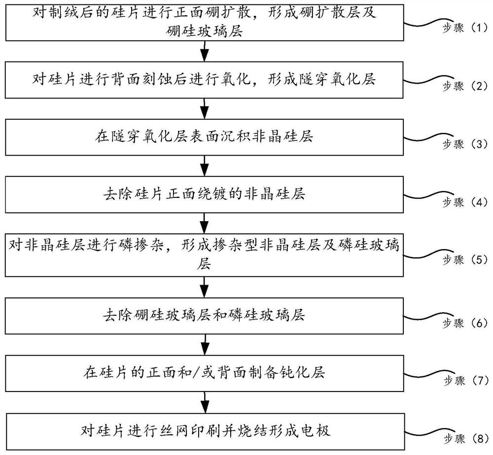
[0035] figure 1 A flow chart of a method for preparing a solar cell provided in an embodiment of the present application, such as figure 1 As shown, the application provides a solar cell preparation method, comprising the following steps:

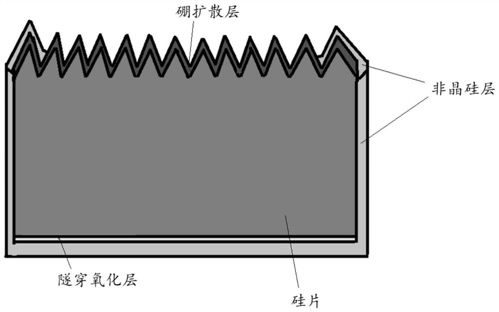
[0036] Step (1): performing boron diffusion treatment on the front side of the textured silicon wafer to form a boron diffusion layer and a borosilicate glass (BSG) layer;

[0037] Step (2): performing back etching on the silicon wafer and then oxidizing to form a tunnel oxide layer;

[0038] Step (3): Depositing an amorphous silicon layer on the surface of the tunnel oxide layer;

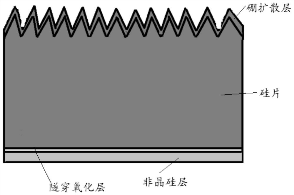
[0039] Step (4): removing the amorphous silicon layer coated on the front side of the silicon wafer;

[0040] Step (5): Doping the amorphous silicon layer with phosphorus to form a doped amorphous silicon layer and a phosphosilicate glass layer (PSG), and the doped amorphous silicon layer and the tunnel oxide layer form a TopCon structure;

[0041] Step (6) ...

Embodiment 1

[0067] Step (0): Texturing the front and back of the N-type crystalline silicon wafer;

[0068] Step (1): performing boron diffusion treatment on the front side of the silicon wafer to form a boron diffusion layer and a borosilicate glass (BSG) layer. At this time, the boron diffusion process will activate the doped boron atoms, making the silicon wafer change from microcrystalline phase to polycrystalline silicon phase.

[0069] Step (2): After etching the back side of the silicon wafer, it is oxidized by a low-pressure chemical vapor deposition method to form a tunnel oxide layer. Specifically, the raw material of the tunneling oxide layer is silicon dioxide, and the thickness of the tunneling oxide layer is 2 nm.

[0070] Step (3): Depositing an amorphous silicon layer on the surface of the tunnel oxide layer, the deposition temperature of the amorphous silicon is 550° C., and the thickness of the amorphous silicon layer is 150 nm;

[0071] Step (4): Clean the silicon waf...

Embodiment 2

[0077] Step (0): Texturing the front and back of the N-type crystalline silicon wafer;

[0078] Step (1): performing boron diffusion treatment on the front side of the silicon wafer to form a boron diffusion layer and a borosilicate glass (BSG) layer. At this time, the boron diffusion process will activate the doped boron atoms, making the silicon wafer change from microcrystalline phase to polycrystalline silicon phase.

[0079] Step (2): After etching the back side of the silicon wafer, it is oxidized by a low-pressure chemical vapor deposition method to form a tunnel oxide layer. Specifically, the raw material of the tunneling oxide layer is silicon dioxide, and the thickness of the tunneling oxide layer is 1 nm.

[0080] Step (3): Depositing an amorphous silicon layer on the surface of the tunnel oxide layer, the deposition temperature of the amorphous silicon is 560° C., and the thickness of the amorphous silicon layer is 120 nm;

[0081] Step (4): Use the prepared mixe...


PUM


Abstract

The invention relates to the photovoltaic field and provides a solar cell and a preparation method thereof. The method comprises the following steps: (1) carrying out the front boron diffusion of a textured silicon wafer, and forming a boron diffusion layer and borosilicate glass; (2) etching the back surface of the silicon wafer and then oxidizing to form a tunneling oxide layer; (3) depositing an amorphous silicon layer on the surface of the tunneling oxide layer; (4) removing the amorphous silicon layer wound and plated on the front surface of the silicon wafer; (5) performing phosphorus doping on the amorphous silicon layer to form a doped amorphous silicon layer and a phosphorosilicate glass layer; and (6) removing the borosilicate glass layer and the phosphorosilicate glass layer. According to the solar cell and the preparation method thereof, the over-etching phenomenon generated by winding-plating removing treatment can be effectively reduced.

Description

technical field [0001] The present application relates to the technical field of photovoltaic cells, in particular, to a solar cell and a preparation method thereof. Background technique [0002] As an important part of the new energy industry, photovoltaic modules have been widely used due to their flexible power generation methods and strong environmental adaptability. [0003] Tunnel Oxide Passivated Contact (TOPCon, Tunnel Oxide Passivated Contact) technology is a new type of silicon solar cell technology. Specifically, a layer of ultra-thin (about 1.5nm) silicon oxide is first prepared on the back of the cell, and then a layer of Doped amorphous silicon layer, the two together form a passivation contact structure, these two layers of material provide a good surface passivation for the back of the silicon wafer, because the oxide layer is very thin, the doped amorphous silicon layer is not suitable for many Said to have good conductivity, many carriers can penetrate the...

Claims


Application Information

Patent Timeline
IPC IPC(8): H01L31/18H01L31/0216
CPCH01L31/1876H01L31/1804H01L31/02167Y02E10/547Y02P70/50
Inventor 熊诗龙金井升
Owner ZHEJIANG JINKO SOLAR CO LTD
Why Eureka
Try Eureka