A method for preparing graphene single crystal wafer on copper-based textured film substrate

A technology of graphene and single crystal, which is applied in the field of preparing graphene single crystal wafers on copper-based textured film substrates, can solve the problems of high cost, achieve the effects of reducing production costs, achieving wide application, and consistent orientation

Active Publication Date: 2022-07-05
SHANGHAI INST OF MICROSYSTEM & INFORMATION TECH CHINESE ACAD OF SCI
View PDF5 Cites 0 Cited by
  • Summary
  • Abstract
  • Description
  • Claims
  • Application Information

AI Technical Summary

Problems solved by technology

[0003] The purpose of the present invention is to provide a method for preparing graphene single crystal wafers on a copper-based textured film substrate, thereby solving the problem of high cost caused by epitaxial growth of single crystal graphene wafers on single crystal substrates in the prior art question

Method used


Image

  • A method for preparing graphene single crystal wafer on copper-based textured film substrate
  • A method for preparing graphene single crystal wafer on copper-based textured film substrate
  • A method for preparing graphene single crystal wafer on copper-based textured film substrate

Examples


Embodiment 1

[0032] A 800nm ​​copper-based textured film was deposited on the sapphire surface by magnetron sputtering at room temperature, in which copper was the main element, nickel was the auxiliary element, and the content of nickel was 15%. preparation. Then, the copper-based textured film substrate was placed in a chemical vapor deposition system, and annealed in a protective atmosphere of argon and hydrogen. The flow ratio of argon and hydrogen was 300sccm:80sccm, the annealing temperature was 1000 °C, and the annealing time was After 60 minutes, 10 sccm of methane was introduced, and the graphene film was grown at a temperature of 1000° C. for 10 minutes, so that a graphene single crystal wafer was epitaxially grown on the surface of the copper-based textured film substrate.

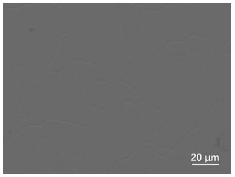
[0033] figure 1 It is an optical microscope topography of graphene on the surface of the copper-based textured film. It can be seen from the figure that the surface is flat except for the substrate grain bo...

Embodiment 2

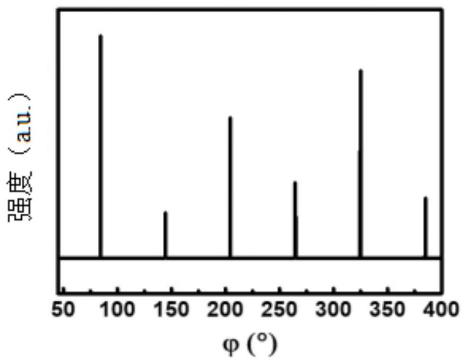
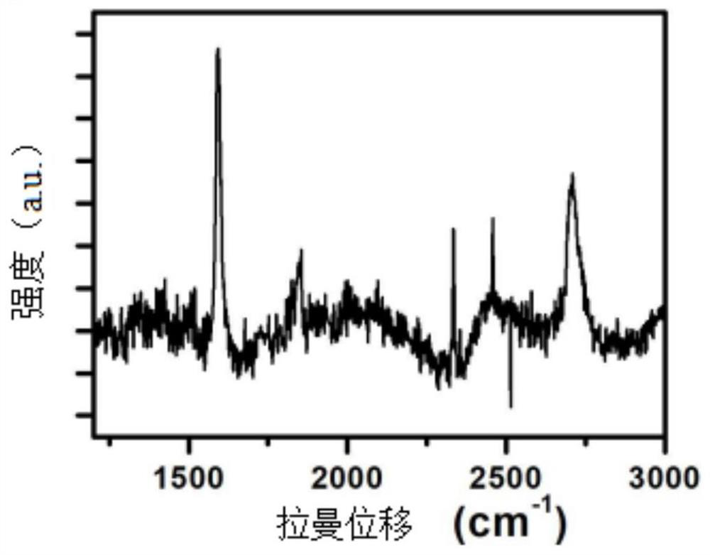
[0035] The difference between this embodiment and the first embodiment is that the content of nickel element in the copper-based textured film substrate prepared in the first embodiment is adjusted from 15% to 10%, the flow ratio of argon gas and hydrogen gas is 200sccm:50sccm, and the annealing The temperature is 800°C, the annealing time is 100min, the growth temperature of the graphene film is 300°C, and other process parameters are the same as those in the first embodiment. like Figure 7 shown, by analyzing the Raman spectrum inside the crystalline domain, at ~1600 cm -1 With ... 2700cm -1 Graphene characteristic peaks appear at the Graphene, and there is no defect peak, which confirms that the grown graphene is of high quality. like Figure 8 As shown, the LEED diffraction spot of the graphene on the surface of the copper-nickel alloy film in Example 2 shows that the orientation of the graphene is consistent, and it is a single crystal film.

Embodiment 3

[0037] The difference between this embodiment and Embodiment 1 is that the content of nickel element in the copper-based textured film substrate in Embodiment 1 is adjusted to 5%, the flow ratio of argon and hydrogen gas is 100sccm:20sccm, and the annealing temperature is 500°C. The annealing time was 120 min, the growth temperature of the graphene film was 500° C., and other process parameters were the same as those in the first embodiment. like Figure 9 shown, by analyzing the Raman spectrum inside the crystalline domain, at ~1600 cm -1 With ... 2700cm -1 Graphene characteristic peak appears at the place, and no defect peak of graphene is observed, which confirms that the quality of the grown graphene is high; Figure 10 This is the LEED diffractogram of the graphene on the surface of the alloy textured film in this example. The result shows that the orientation of the graphene on the copper-nickel textured surface is consistent, and it is a single crystal film.


PUM

PropertyMeasurementUnit
thicknessaaaaaaaaaa

Abstract

The present invention provides a method for preparing a graphene single crystal wafer on a copper-based textured film substrate, comprising the following steps: S1: providing a copper-based textured film substrate, and applying the copper-based textured film substrate to the Putting in a chemical vapor deposition system for annealing treatment; and S2: feeding a gaseous carbon source to epitaxially grow a graphene single crystal wafer on the surface of the copper-based textured film substrate. According to a method for preparing a graphene single crystal wafer on a copper-based textured film substrate provided by the present invention, the problem of high cost caused by epitaxial growth of a single crystal graphene wafer on a single crystal substrate is solved, which is beneficial to graphene The large-scale application of single crystal wafers is of great significance to the realization of the wide application of graphene in the field of microelectronics.

Description

technical field [0001] The invention belongs to the field of material preparation, and more particularly relates to a method for preparing a graphene single crystal wafer on a copper-based textured film substrate. Background technique [0002] Graphene has excellent optoelectronic properties and shows great application potential in various fields, which has attracted wide attention from all walks of life. Among the many applications of graphene, the most attractive one is in the field of microelectronics. Graphene as a channel material is an important candidate material to replace existing silicon materials due to its ultra-high carrier mobility and is expected to continue Moore's Law. Among them, the batch preparation of graphene single crystal wafers is the premise for its large-scale application in the field of microelectronics in the future. The preparation of existing graphene single crystal wafers mainly uses metal single crystals or germanium single crystals as subs...

Claims


Application Information

Patent Timeline
Patent Type & Authority Patents(China)
IPC IPC(8): C30B25/18C30B29/02C23C14/35C23C14/18
CPCC30B25/186C30B29/02C23C14/35C23C14/185Y02P70/50
Inventor 张学富吴天如王浩敏于庆凯谢晓明
Owner SHANGHAI INST OF MICROSYSTEM & INFORMATION TECH CHINESE ACAD OF SCI
Why Eureka
Try Eureka