A kind of substrate material, Raman surface enhancement substrate, preparation method, application
A technology of base material and surface enhancement, applied in the fields of analyzing materials, Raman scattering, material excitation analysis, etc., can solve the problem of low work efficiency, and achieve the effect of improving work efficiency, simple preparation method and broad market prospect.
- Summary
- Abstract
- Description
- Claims
- Application Information
AI Technical Summary
Problems solved by technology
Method used
Image
Examples
Embodiment 1
[0041] A Raman surface enhanced substrate, the specific preparation method is as follows:
[0042] 1) Remove impurities on the surface of the material: cut the cast magnesium ingot into 15×15×4mm 3 The rectangular blocks were anodized. Before the treatment, all the samples were ground with 1200-grit silicon carbide abrasive paper, and then washed with ethanol and deionized water in sequence to remove surface impurities to obtain magnesium rectangular blocks after removal of impurities.
[0043] 2) Pretreatment: The electrolyte in the anodizing process is selected as KOH containing 2g / L and Na 10g / L prepared in deionized water. 3 PO 4 The mixed solution of the magnesium rectangle block and the carbon tube after removing impurities are respectively used as the anode and the cathode in the anodizing process, and the positions of the anode and the cathode are adjusted respectively so that the carbon tube is directly opposite to and parallel to the surface of the magnesium rectangle...
Embodiment 2
[0046] In order to study the influence of surface conditions (such as porosity and roughness) on the strength of SERS (Surface-Enhanced Raman Scattering, surface-enhanced Raman), the anodizing treatment time is taken as the single variable, so the power-on time is 1min, 2min and 5min respectively. Ultimately, the experimental results need to be compared with anodization treatment energization time and gold film thickness as variables to obtain the substrate that can produce the best Raman-enhanced signal.
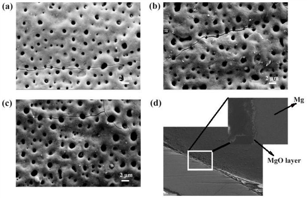
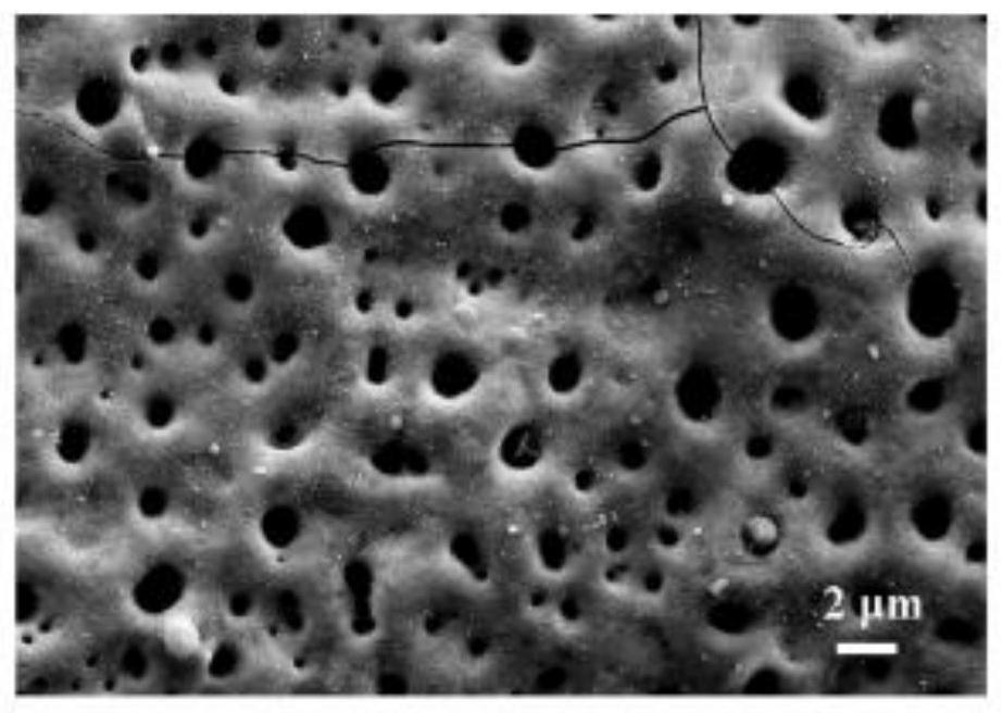
[0047] In this example, the Raman surface-enhanced substrates prepared with different energization times in Example 1 were subjected to SEM characterization, and the specific SEM characterization results are as follows figure 1 As shown, among them, figure 1 The SEM images of the Raman surface-enhanced substrates prepared for different energization times provided in this example, in figure 1 Among them, picture (a), picture (b) and picture (c) are the SEM images of the Ram...
Embodiment 3
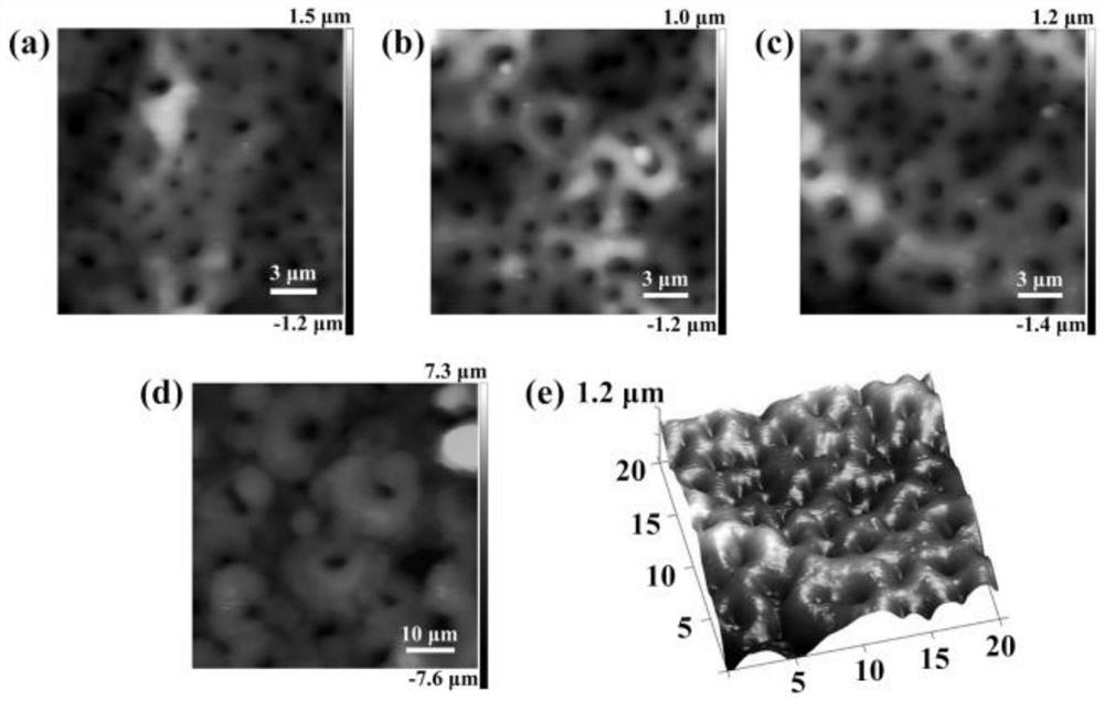
[0049] In order to further observe the geometric parameters of the Raman surface-enhanced substrates prepared with different energization times in Example 1, detailed characterization was carried out by AFM. image 3 AFM images of Raman surface-enhanced substrates prepared for different energization times provided in Examples of the present invention. exist image 3 Among them, picture (a), picture (b), picture (c) and picture (d) are the AFM images of the Raman surface-enhanced substrate when the energization time (that is, the corrosion time) is 1min, 2min, 5min, and 10min, respectively. Figure (e) is a three-dimensional image of the Raman surface-enhanced substrate when the energization time (ie, corrosion time) is 5 minutes. from image 3 It can be seen from the image 3 The radius and depth of the circular hole in (a) are 0.7±0.25 μm and 0.5±0.16 μm, respectively; image 3 The radius and depth of the circular hole in (b) are 0.9 ± 0.3 μm and 6 ± 0.15 μm, respectively;...
PUM
| Property | Measurement | Unit |
|---|---|---|
| concentration | aaaaa | aaaaa |
| concentration | aaaaa | aaaaa |
| particle size | aaaaa | aaaaa |
Abstract
Description
Claims
Application Information
 - R&D
- Intellectual Property
- Life Sciences
- Materials
- Tech Scout
- Unparalleled Data Quality
- Higher Quality Content
- 60% Fewer Hallucinations
Browse by: Latest US Patents, China's latest patents, Technical Efficacy Thesaurus, Application Domain, Technology Topic, Popular Technical Reports.
© 2025 PatSnap. All rights reserved.Legal|Privacy policy|Modern Slavery Act Transparency Statement|Sitemap|About US| Contact US: help@patsnap.com


