Preparation method of nanosheet array electrocatalyst
A technology of nanosheet array and electrocatalyst, which is applied in the field of electrochemistry, can solve the problem of less water splitting reaction of binary metal selenide, and achieve the effect of easy large-scale production, large-scale production, and improvement of embrittlement
- Summary
- Abstract
- Description
- Claims
- Application Information
AI Technical Summary
Problems solved by technology
Method used
Image
Examples
Embodiment 1
[0026] The preparation of nanosheet array NiCoSe@NF1 includes the following steps:
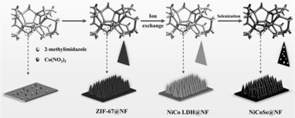
[0027] 1) Preparation of nanosheet array ZIF-67@NF:
[0028] 11) Pretreatment of foamed nickel, the foamed nickel is cleaned before use, ultrasonicated with 3.0M hydrochloric acid, acetone and water respectively for 20 minutes, then rinsed several times with absolute ethanol, dried at 60°C for 6 hours, and the pretreated foam is obtained nickel.
[0029] 12) Disperse 1.3136g of 2-methylimidazole and 0.582g of cobalt nitrate hexahydrate (the corresponding molar number at this time is 0.2mmol) in 40ml of deionized water, stir magnetically for 10min, and quickly pour 2-methylimidazole into Co(NO 3 ) 2 ·6H 2 In the O solution, the transparent solution quickly turned blue-purple, and continued to stir for 5 minutes.
[0030] 13) Put a piece of 2*4cm -2 The nickel foam was put into it, and after standing for 4 hours, it was washed several times with deionized water and absolute ethanol, and dr...
Embodiment 2
[0034] For the preparation of nanosheet array NiCoSe@NF2, the amount of selenium powder in step 3) in Example 1 was changed to 2 mmoles of selenium powder, and the amounts of other steps and components were kept unchanged to obtain nanosheet array NiCoSe@NF2.
[0035] For the preparation of nanosheet array NiCoSe@NF3, the amount of selenium powder in step 3) in Example 1 was changed to 4 mmoles of selenium powder, and the amounts of other steps and components were kept unchanged to obtain nanosheet array NiCoSe@NF3.
[0036] For the preparation of nanosheet array NiCoSe@NF4, the amount of selenium powder in step 3) in Example 1 was changed to 6 mmoles of selenium powder, and the amounts of other steps and components were kept unchanged to obtain nanosheet array NiCoSe@NF4.
[0037] For the preparation of nanosheet array NiCoSe@NF5, the amount of selenium powder in step 3) in Example 1 was changed to 8 mmoles of selenium powder, and the amounts of other steps and components were...
Embodiment 3
[0040] Embodiment 3 performance test
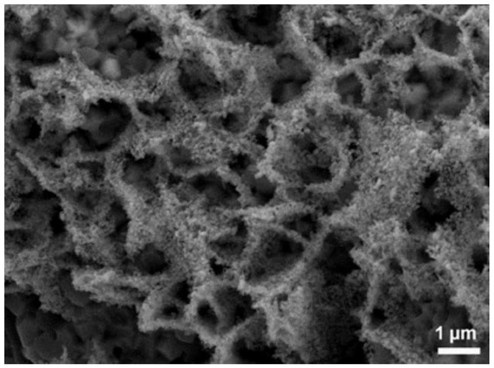
[0041] 1. The nanosheet array NiCoSe@NF2 was characterized by scanning electron microscopy, and the field emission scanning electron microscopy (FESEM) image analysis was carried out on a 10.0kV JEOLJ SM-7800F. The results are as follows figure 2 shown. From figure 2 It can be seen that NiCoSe nanosheets with uniform size grow on the surface of nickel foam, which becomes thinner than the thickness of precursor nanosheets, which is more conducive to the penetration of electrolyte and the improvement of electrochemical properties.
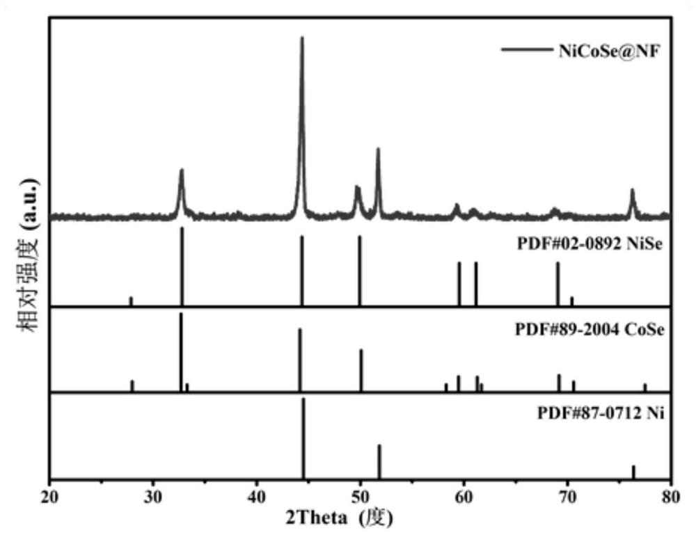
[0042] 2. Use the Cu target radiation source of Mac Science MXP-18 X-ray diffractometer to conduct X-ray diffraction on the nanosheet array NiCoSe@NF2, the results are as follows image 3 shown. image 3 is the X-ray diffraction pattern of the nanosheet array NiCoSe@NF2 of the present invention. It can be seen from the figure that the target product contains the diffraction peaks of NiSe, CoSe and Ni at th...
PUM
 Abstract
Description
Claims
Application Information
 - R&D
- Intellectual Property
- Life Sciences
- Materials
- Tech Scout
- Unparalleled Data Quality
- Higher Quality Content
- 60% Fewer Hallucinations
Browse by: Latest US Patents, China's latest patents, Technical Efficacy Thesaurus, Application Domain, Technology Topic, Popular Technical Reports.
© 2025 PatSnap. All rights reserved.Legal|Privacy policy|Modern Slavery Act Transparency Statement|Sitemap|About US| Contact US: help@patsnap.com


