Silicon-based micro-cavity narrow-band near-infrared photoelectric detector

A near-infrared optical and electrical detector technology, which is applied to circuits, electrical components, semiconductor devices, etc., can solve the problems of high cost, complicated detector preparation methods, and difficult integration of electronic devices, etc., and achieve low cost, high-efficiency detection, and response fast effect

Active Publication Date: 2020-11-27
HEFEI UNIV OF TECH
View PDF6 Cites 5 Cited by
  • Summary
  • Abstract
  • Description
  • Claims
  • Application Information

AI Technical Summary

Problems solved by technology

JunfengSong et al. proposed a photodetector based on a microring resonator. The length of the photodetector is only 4 μm. When working in the L-band, the microring resonator increases the responsivity of this detector by about 2 times, but The preparation method of the detector is complicated, it is not easy to integrate with electronic devices and the cost is high [J.Song; Andy Lim; et al.Optics express.2014,22,26976-26984.]

Method used


Image

  • Silicon-based micro-cavity narrow-band near-infrared photoelectric detector
  • Silicon-based micro-cavity narrow-band near-infrared photoelectric detector
  • Silicon-based micro-cavity narrow-band near-infrared photoelectric detector

Examples


Embodiment 1

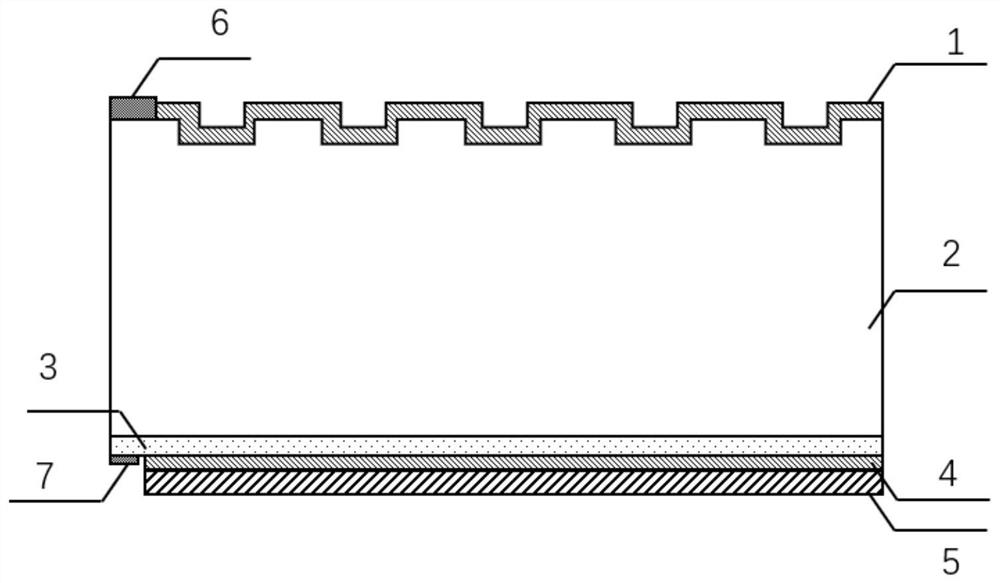
[0025] Such as figure 1 As shown, the silicon-based microcavity narrow-band near-infrared photodetector of this embodiment uses a single crystal silicon substrate 2 as a base, and the upper surface of the single crystal silicon substrate 2 is etched into a silicon microhole array structure. An upper insulating layer 1 is provided on the hole array; a layer of graphene film 3 is transferred on the lower surface of the single crystal silicon substrate 2 to form a graphene-silicon Schottky heterojunction; a lower surface is provided on the lower surface of the graphene film 3 An insulating layer 4; a metal reflective layer 5 is provided on the lower surface of the lower insulating layer 4;

[0026] Top electrode 6 is arranged on the upper surface of monocrystalline silicon substrate 2, and bottom electrode 7 is arranged on the lower surface of graphene film 3, and top electrode 6 forms ohmic contact with monocrystalline silicon substrate 2, and bottom electrode 7 and graphene Th...

Embodiment 2

[0041] Such as figure 1 As shown, the silicon-based microcavity narrow-band near-infrared photodetector of this embodiment uses a single crystal silicon substrate 2 as a base, and the upper surface of the single crystal silicon substrate 2 is etched into a silicon microhole array structure. An upper insulating layer 1 is provided on the hole array; a layer of graphene film 3 is transferred on the lower surface of the single crystal silicon substrate 2 to form a graphene-silicon Schottky heterojunction; a lower surface is provided on the lower surface of the graphene film 3 An insulating layer 4; a metal reflective layer 5 is provided on the lower surface of the lower insulating layer 4;

[0042] Top electrode 6 is arranged on the upper surface of monocrystalline silicon substrate 2, and bottom electrode 7 is arranged on the lower surface of graphene film 3, and top electrode 6 forms ohmic contact with monocrystalline silicon substrate 2, and bottom electrode 7 and graphene Th...


PUM

PropertyMeasurementUnit
thicknessaaaaaaaaaa
diameteraaaaaaaaaa
thicknessaaaaaaaaaa

Abstract

The invention discloses a silicon-based micro-cavity narrow-band near-infrared photoelectric detector. In the structure of the detector, a monocrystalline silicon substrate is used as a base; whereinthe upper surface of the monocrystalline silicon substrate is etched into a silicon micropore array structure; an upper insulating layer is arranged on the silicon micropore array; a graphene film istransferred on the lower surface of the monocrystalline silicon substrate to form a graphene-silicon Schottky heterojunction; a lower insulating layer and a metal reflecting layer are sequentially arranged on the lower surface of the graphene film. The detector prepared by the invention realizes visible light blind narrowband near-infrared response, has the advantages of high response speed, easyintegration and the like, and also has the advantages of simple preparation method, low cost, high stability, strong compatibility and the like.

Description

technical field [0001] The invention relates to a silicon-based microcavity narrow-band near-infrared photodetector, which belongs to the technical field of semiconductor photoelectric devices. Background technique [0002] Traditional infrared photoelectric detection plays a vital role in the fields of military, remote sensing, communication, life science, and space exploration. In recent years, artificial intelligence, big data, and smart cities have demanded infrared information detection and intelligent perception Increasingly intense, narrow-band response and high-sensitivity near-infrared photodetectors have great application value in the fields of spectroscopy, clinical medicine, imaging, and chemical element analysis. Currently, narrow-band photodetectors are usually implemented using the following three methods: 1) Combining broadband photodetectors with bandpass filters, this method requires high-cost filters, complex optical system integration and design, and incr...

Claims


Application Information

Patent Timeline
Patent Type & Authority Applications(China)
IPC IPC(8): H01L31/108H01L31/028H01L31/0216H01L31/0232
CPCH01L31/108H01L31/028H01L31/02161H01L31/0232Y02P70/50
Inventor 于永强宋龙梅夏宇刘佳杨许高斌马渊明陈士荣
Owner HEFEI UNIV OF TECH
Why Eureka
Try Eureka