

P-type semiconductor graphite and preparation method thereof
A semiconductor and graphite technology, which is applied in the field of P-type semiconductor graphite and its preparation, can solve the problems of poor corrosion resistance and achieve the effects of improving hardness and corrosion resistance, good stability, and improving corrosion resistance
- Summary
- Abstract
- Description
- Claims
- Application Information
AI Technical Summary
Problems solved by technology
Method used
Image

Examples
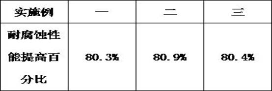
Embodiment 1
[0032] The present invention proposes a P-type semiconductor graphite and a preparation method thereof, including the following raw materials in parts by weight: copper foil, 10 parts of methane, 10 parts of hydrogen gas, 15 parts of boron source gas, 5 parts of polytetrafluoroethylene, and 5 parts of silicon dioxide. 1 part, 1 part of titanium dioxide, 1 part of aluminum oxide, 5 parts of polyurethane;
[0033] Its preparation method comprises the following steps:
[0034] S1: Put the copper foil in the reactor, evacuate, and pass through the argon protective gas, hydrogen and methane, and react for 5 minutes to form a part of the graphene film;
[0035] S2: Then pass the mixed gas of boron source gas and hydrogen into the reactor, and react for 10-30min to obtain boron-doped P-type semiconductor graphene;
[0036] S3: Put polytetrafluoroethylene, silicon dioxide, titanium dioxide, aluminum oxide, and polyurethane into the mixing equipment, stir and mix, the stirring speed i...
Embodiment 2
[0039] The present invention proposes a P-type semiconductor graphite and a preparation method thereof, including the following raw materials in parts by weight: copper foil, 12 parts of methane, 12 parts of hydrogen gas, 17 parts of boron source gas, 7 parts of polytetrafluoroethylene, and 7 parts of silicon dioxide. 3 parts of titanium dioxide, 3 parts of aluminum oxide, 7 parts of polyurethane;
[0040] Its preparation method comprises the following steps:
[0041] S1: Put the copper foil in the reactor, evacuate, and pass through the argon protective gas, hydrogen and methane, and react for 10 minutes to form a part of the graphene film;
[0042] S2: Then pass the mixed gas of boron source gas and hydrogen into the reactor, and react for 20 minutes to obtain boron-doped P-type semiconductor graphene;
[0043] S3: Put polytetrafluoroethylene, silicon dioxide, titanium dioxide, aluminum oxide, and polyurethane into the mixing equipment, stir and mix, the stirring speed is 3...
Embodiment 3
[0046] The present invention proposes a P-type semiconductor graphite and a preparation method thereof, comprising the following raw materials in parts by weight: copper foil, 15 parts of methane, 15 parts of hydrogen gas, 20 parts of boron source gas, 10 parts of polytetrafluoroethylene, and 10 parts of silicon dioxide. 5 parts of titanium dioxide, 5 parts of aluminum oxide, 10 parts of polyurethane;
[0047] Its preparation method comprises the following steps:
[0048] S1: Put the copper foil in the reactor, evacuate, and pass through the argon protective gas, hydrogen and methane, and react for 20 minutes to form a part of the graphene film;
[0049] S2: Then pass the mixed gas of boron source gas and hydrogen into the reactor, and react for 30 minutes to obtain boron-doped P-type semiconductor graphene;
[0050] S3: Put polytetrafluoroethylene, silicon dioxide, titanium dioxide, aluminum oxide, and polyurethane into the mixing equipment, stir and mix, the stirring speed ...
PUM
 Abstract
Description
Claims
Application Information