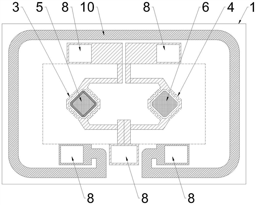
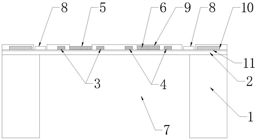
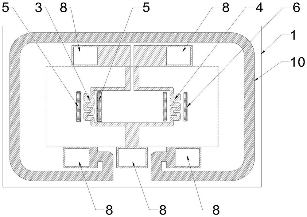
Indirectly-heated silicon-based film catalytic hydrogen sensor and processing method thereof
A silicon-based thin-film, side-heating technology, applied in the field of hydrogen sensors, can solve the problems of hydrogen sensor selectivity, safety and stability, weak sensitivity output signal, stability and service life need to be further improved, and the specific surface area of porous ceramics decreases, etc. problem, achieve the effect of reducing cross-interference, improving stability and reliability, and reducing thermal shock
- Summary
- Abstract
- Description
- Claims
- Application Information
AI Technical Summary
Problems solved by technology
Method used
Image
Examples
Embodiment 1
[0059] A processing method for side-heated silicon-based thin film catalytic hydrogen sensors, comprising the following steps:
[0060] S1: Clean the silicon substrate with standard RCA process and dry it with nitrogen gas;
[0061] S2: Deposit a silicon nitride layer on the cleaned silicon substrate 1 by a low-pressure chemical vapor deposition method, and then deposit a silicon dioxide layer on the surface of the silicon nitride layer by a plasma-enhanced chemical vapor deposition method to obtain a heat insulating layer 2;
[0062] S3: On the substrate obtained in S2, a layer of high-temperature buffer layer 11 is deposited on the surface of the heat-insulating layer 2 obtained in step S2 by magnetron sputtering;
[0063] S4: On the substrate obtained in S3, perform coating, photolithography, and development treatments, and use magnetron sputtering or deposition to deposit a material layer with a high temperature coefficient of resistance, and use the lift-off process to ob...
Embodiment 2
[0070] A processing method for side-heated silicon-based thin film catalytic hydrogen sensors, comprising the following steps:
[0071] S1: Cleaning the silicon substrate 1 by using a standard RCA process, and drying it with nitrogen gas;
[0072] S2: Deposit a silicon nitride layer on the cleaned silicon substrate 1 by a low-pressure chemical vapor deposition method, and then deposit a silicon dioxide layer on the surface of the silicon nitride layer by a plasma-enhanced chemical vapor deposition method to obtain a heat insulating layer 2;
[0073] S3: On the substrate obtained in S2, deposit a high-temperature buffer layer 11 on the surface of the heat insulating layer 2 obtained in step S2 by thermal evaporation deposition;
[0074] S4: On the substrate obtained in S3, perform coating, photolithography, and development treatments, and use the deposition method in step S3 to deposit a material layer with a high temperature coefficient of resistance, and use the lift-off proc...
PUM
| Property | Measurement | Unit |
|---|---|---|
| diameter | aaaaa | aaaaa |
Abstract
Description
Claims
Application Information


