


Quick Research
Generate reliable direction feasibility study reports for your R&D in just a few steps.

Technical Q&A
Discover and master advanced knowledge NOW. Basics, ideas, possibilities, all at once.

Find Solutions
As an expert in R&D theories, this can generate solutions to your technical problems instantly.

Evaluate Feasibility
Analyze your overall solution with one click, know your potential R&D risks in advance.

Monitor Landscape
Get weekly tech updates, stay abreast of the latest tech innovations and key insights.
Graphene OLED device and preparation method thereof
A graphene and device technology, applied in the field of graphene OLED devices and their preparation, can solve the problems of low power consumption, poor luminous efficiency and stability, weak affinity, etc., to improve electrical conductivity, improve injection efficiency, and improve performance effect
- Summary
- Abstract
- Description
- Claims
- Application Information
AI Technical Summary
Problems solved by technology
Method used
Image

Examples
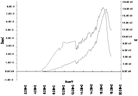
Embodiment 1
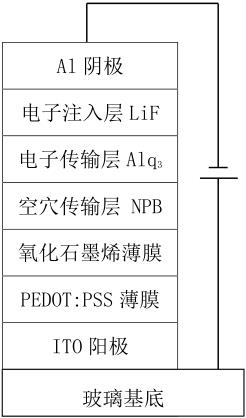
[0030] A graphene OLED device, the structure of the OLED device includes from bottom to top: glass substrate, ITO anode, PEDOT:PSS film layer, graphene oxide film layer, hole transport layer NPB, electron transport layer Alq3, electron injection layer LiF and Al cathode.
[0031] The invention is a stacked OLED device, the brightness and current efficiency of the device can be changed with the stacked light-emitting units, and the stacked OLED device can also realize high brightness at low current density, avoid leakage current and electric field breakdown, and realize long life of the device .
[0032] The glass substrate is smooth and flat, and the rough substrate will cause the anode to appear uneven, which is prone to short circuit of the device, resulting in irreparable damage.
[0033] Diffusion of metal in the ITO electrode to the organic layer is an important reason for the decline of OLED efficiency and stability. Adding a modification layer between the electrode and...
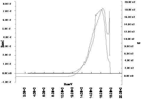
Embodiment 2
[0045] A graphene OLED device, the structure of the OLED device includes from bottom to top: glass substrate, ITO anode, PEDOT:PSS film layer, two layers of graphene oxide film layer, hole transport layer NPB, electron transport layer Alq3, electron injection layer LiF and Al cathode.
Embodiment 3
[0047] A graphene OLED device, the structure of the OLED device includes from bottom to top: glass substrate, ITO anode, PEDOT:PSS film layer, three layers of graphene oxide film layer, hole transport layer NPB, electron transport layer Alq3, electron injection layer LiF and Al cathode.
PUM
| Property | Measurement | Unit |
|---|---|---|
| area | aaaaa | aaaaa |
| thickness | aaaaa | aaaaa |
| luminance | aaaaa | aaaaa |
Abstract
Description
Claims
Application Information
 - R&D Engineer
- R&D Manager
- IP Professional
- Industry Leading Data Capabilities
- Powerful AI technology
- Patent DNA Extraction
Browse by: Latest US Patents, China's latest patents, Technical Efficacy Thesaurus, Application Domain, Technology Topic, Popular Technical Reports.
© 2024 PatSnap. All rights reserved.Legal|Privacy policy|Modern Slavery Act Transparency Statement|Sitemap|About US| Contact US: help@patsnap.com