N-type high-efficiency solar cell and preparation method

A solar cell, N-type technology, applied in the field of solar cells, can solve the problems that the efficiency and yield of heterojunction solar cells are greatly affected, and achieve the effects of promoting the application of industrialization, reducing production costs, and low cost

Active Publication Date: 2021-01-29
CHANGZHOU SHICHUANG ENERGY CO LTD
View PDF4 Cites 9 Cited by
  • Summary
  • Abstract
  • Description
  • Claims
  • Application Information

AI Technical Summary

Problems solved by technology

[0003] Due to the presence of metal impurities in solar-grade Czochralski monocrystalline silicon rods, mainly transition metal impurities, deep-level recombination centers or metal precipitation will be formed. However, there is no high-temper

Method used


Image

  • N-type high-efficiency solar cell and preparation method
  • N-type high-efficiency solar cell and preparation method

Examples


preparation example Construction

[0034] The preparation method of the N-type high-efficiency heterojunction solar cell of the present invention first performs gettering treatment on the N-type silicon wafer, and then completes the conventional production of the solar cell, and the gettering treatment includes the following steps:

[0035] (1) Clean the silicon wafer;

[0036] (2) Coating or depositing a layer of gettering source on the front and back of the silicon wafer;

[0037] (3) The silicon wafer coated or deposited with the gettering source is heat-treated in a chain annealing furnace to complete the gettering, and a gettering layer is formed on the surface of the silicon wafer;

[0038] (4) Erosion removes the gettering layer on the surface of the silicon wafer.

[0039] As another preferred solution of the present invention, step (4) can also remove the gettering layers on the front and back of the silicon wafer in the subsequent texturing process of conventional battery production, which further si...

Embodiment 1

[0043] (101) Take an N-type silicon wafer with the same or close minority carrier lifetime, first wash it with NaOH, then mix it with HF and HCL, and dry it;

[0044] (102) Apply a layer of gettering source on the surface of the silicon wafer by printing, rolling, spraying or spin-coating a liquid source on the front and back of the silicon wafer respectively. The liquid source can be a phosphorus-containing slurry or a boron-containing slurry , in this embodiment, roll-coat phosphoric acid solution on the front and back of the silicon wafer to form a gettering source on the surface of the silicon wafer;

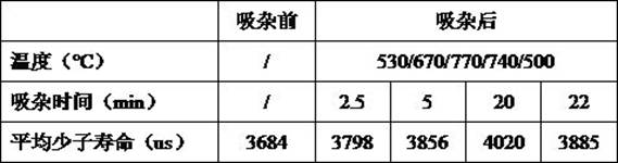
[0045] (103) Send the silicon wafer coated with the gettering source to the chain annealing furnace for heat treatment. The chain annealing furnace is equipped with 5 temperature zones, and the temperature of each temperature zone is respectively set to 530°C, 670°C, and 770°C , 740°C, and 500°C, divided into four groups, and heat-treated in a chain annealing furnace for 2.5...

Embodiment 2

[0058] (201) Take an N-type silicon wafer with the same or close minority carrier lifetime, first wash it with NaOH, then mix it with HF and HCL, and dry it;

[0059] (202) Send the silicon wafer into a tubular diffusion furnace, which is filled with nitrogen and oxygen carrying a liquid source, and a layer of gettering source is deposited on the front and back of the silicon wafer through high-temperature diffusion. The liquid source can be Phosphorus oxychloride or boron tribromide, in this embodiment, a layer of boron source is deposited on the surface of the silicon wafer as a gettering layer by high-temperature diffusion of boron tribromide in a tubular diffusion furnace;

[0060] (203) Send the silicon wafer with the gettering source deposited on the surface into the chain-type annealing furnace for gettering treatment. The chain-type annealing furnace is equipped with 5 temperature zones, and the temperature of each temperature zone is set to 530°C, 670°C, 770°C, respect...


PUM


Abstract

The invention discloses an N-type high-efficiency heterojunction solar cell and a preparation method thereof. The N-type high-efficiency heterojunction solar cell is made of an N-type silicon wafer. The preparation method comprises the following steps of: firstly, performing gettering treatment on an N-type silicon wafer, and then completing conventional manufacturing of the heterojunction solar cell. The gettering treatment comprises the following steps: (1) cleaning a silicon wafer; (2) coating or depositing a layer of gettering source on the front surface and the back surface of the siliconwafer; (3) performing heat treatment on the silicon wafer coated or deposited with the gettering source through a chain annealing furnace to finish gettering, and forming a gettering layer on the surface of the silicon wafer; and (4) conducting corroding to remove the gettering layer on the surface of the silicon wafer. According to the invention, the content of metal impurities in the silicon wafer body is reduced, the minority carrier lifetime of the silicon wafer is prolonged, and the conversion efficiency of the cell is finally improved; the cell efficiency distribution is more centralized, and the product consistency is improved; and the cell edge electric leakage rate is reduced, and the cell yield is improved.

Description

technical field [0001] The invention relates to the technical field of solar cells, in particular to an N-type high-efficiency solar cell and a preparation method. Background technique [0002] At present, most crystalline silicon solar cells in the world use the standard process of traditional P-type cells. However, with the gradual development of high-efficiency crystalline silicon cell manufacturing technology, P-type cells are facing capital and technology investment margins after the conversion efficiency reaches more than 22%. Due to the effect of diminishing returns, it is difficult to further improve the conversion efficiency. Therefore, a large number of solar cell manufacturers have begun to focus on the commercialization of N-type solar cells, such as heterojunction (HJT) cells and interdigitated back contact (IBC) cells. Compared with P The higher the type of silicon wafer, it is conducive to the further improvement of battery efficiency. [0003] Due to the pr...

Claims


Application Information

Patent Timeline
IPC IPC(8): H01L31/18H01L31/074H01L31/0288
CPCH01L31/1804H01L31/186H01L31/1864H01L31/0288H01L31/074Y02P70/50
Inventor 任常瑞张佳舟绪欣符黎明
Owner CHANGZHOU SHICHUANG ENERGY CO LTD
Why Eureka
Try Eureka