Fin type photovoltaic silicon-based plasmon hot carrier infrared detection chip and manufacturing method thereof

A technology of plasmons and hot carriers, applied in the field of photoelectric detection, can solve the problems of high dark current, inability to work with silicon materials, low quantum efficiency and low detection rate, and achieve the effect of strong radiation resistance and low cost

Active Publication Date: 2021-02-12
FUDAN UNIV
View PDF6 Cites 1 Cited by
  • Summary
  • Abstract
  • Description
  • Claims
  • Application Information

AI Technical Summary

Problems solved by technology

[0004] The purpose of the present invention is to provide a fin-type photovoltaic silicon-based plasmon hot carrier infrared detection chip and its manufacturing method, so as to solve the problem that silicon materials cannot work due to the band gap limitation and the wave band greater than 1.1 μm, and overcome the current photovoltaic The defects of low responsivity, quantum efficiency and detection rate and high dark current of silicon-based thermionic infrared devices realize high sensitivity and multi-band infrared monitoring capabilities of all-silicon-based photodetectors

Method used


Image

  • Fin type photovoltaic silicon-based plasmon hot carrier infrared detection chip and manufacturing method thereof
  • Fin type photovoltaic silicon-based plasmon hot carrier infrared detection chip and manufacturing method thereof
  • Fin type photovoltaic silicon-based plasmon hot carrier infrared detection chip and manufacturing method thereof

Examples


Embodiment Construction

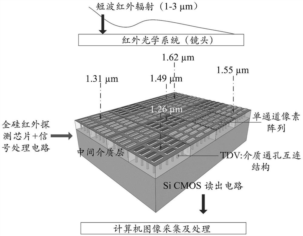
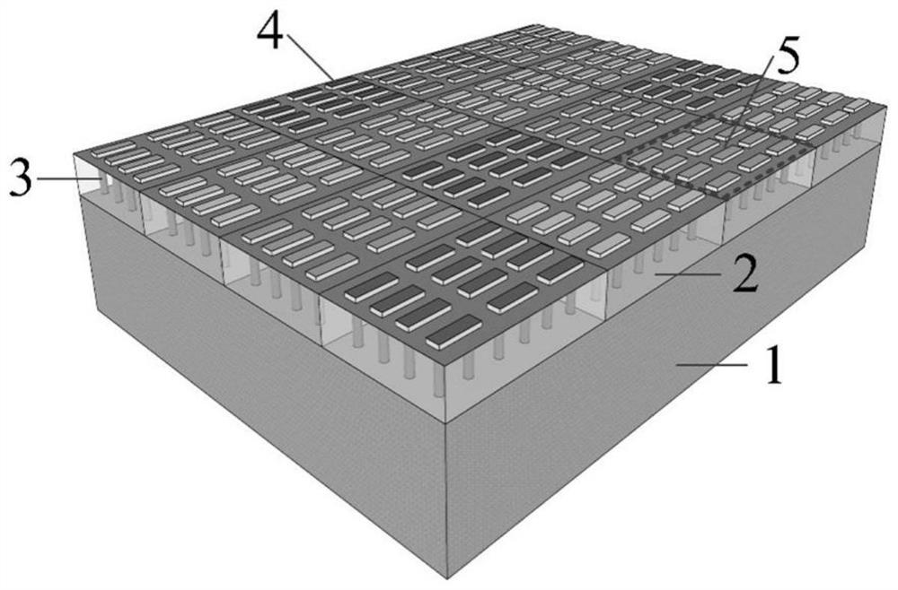
[0064] The present invention will be further described below in conjunction with the accompanying drawings and embodiments. refer to Figure 1-3 As shown, the entire device structure includes:

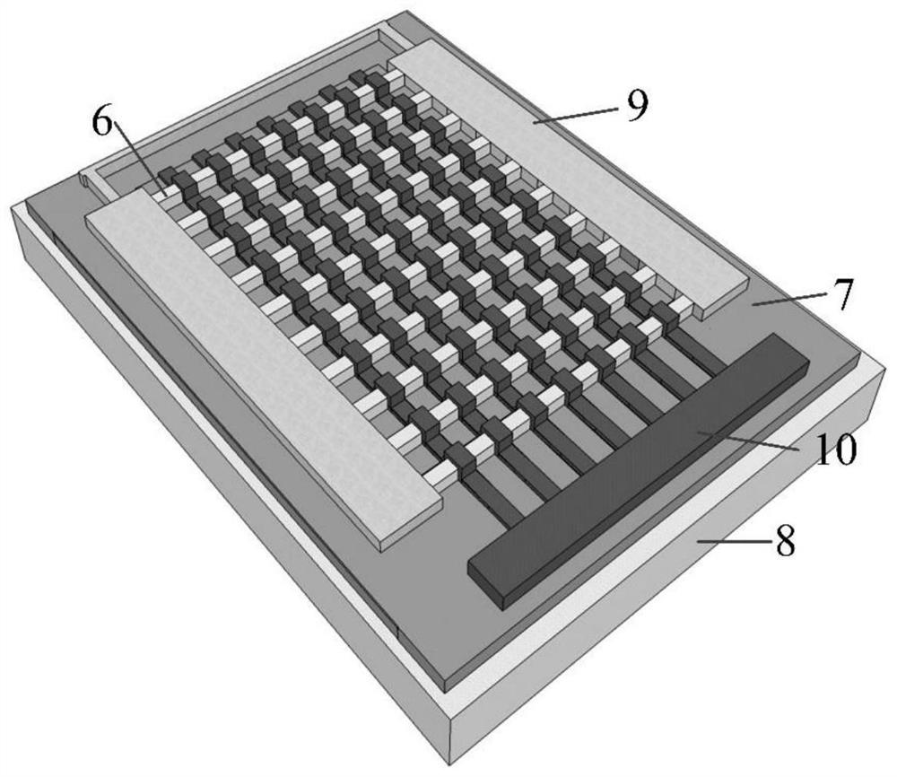
[0065] A silicon-on-insulator (SOI) substrate. The bottom layer of the substrate is a common silicon material used to prepare CMOS signal readout circuits; the middle layer is a dielectric layer, which can integrate through-hole interconnection structures inside; the top layer is a thin A layer of silicon, as an infrared light-sensitive layer, distributes several sub-arrays responding to different single-bands inside it, and single-pixel fin photovoltaic devices distributed in each sub-array. Among them, the single-pixel fin-type photovoltaic device structure, such as image 3 Shown: It consists of a silicon nanowire array with a specific period on the SOI substrate, aluminum electrodes connected at both ends, and a fin-like structure metasurface with a common connection terminal int...


PUM

PropertyMeasurementUnit
thicknessaaaaaaaaaa
thicknessaaaaaaaaaa

Abstract

The invention belongs to the technical field of photoelectric detection, and particularly relates to a fin type photovoltaic silicon-based plasmon hot carrier infrared detection chip and a manufacturing method thereof. The infrared detection chip comprises an SOI substrate, a pixel array manufactured in top silicon of the SOI substrate, a signal reading circuit manufactured in bottom silicon of the SOI substrate and a through hole interconnection structure manufactured in a middle dielectric layer. Each single-image component comprises a metal electrode, a silicon nanowire array and a fin-typeconstruction metasurface integrated on a nanowire, so that perfect absorption of infrared radiation is achieved, absorbed photons are converted into surface plasmon hot carriers to be transferred into a semiconductor, photovoltaic signals are generated, and the detection function is achieved. The detection chip is manufactured by adopting a three-dimensional integration process, an infrared sensing unit and a signal processing unit are vertically stacked, vertical interconnection in the Z direction is realized between layers by utilizing a through hole filling technology, and the monolithic focal plane array detection chip with high density, low power consumption and ultra-large array scale is obtained.

Description

technical field [0001] The invention belongs to the technical field of photoelectric detection, and in particular relates to a fin-type photovoltaic silicon-based plasmon hot carrier infrared detection chip and a manufacturing method thereof. Background technique [0002] The materials currently used in short-wave infrared (1-3μm) photodetection are almost all dominated by III-V / II-VI materials, such as: InGaAs, HgCdTe, InSb, etc. However, these materials have more or less the following defects: high cost of materials, environmental pollution due to high toxicity, extremely complex and unstable material growth and device preparation processes, low temperature work, and inability to realize large area (currently the largest area of ​​GaAs is 6 inches), etc.; the chip structure prepared by it basically consists of two parts: the infrared sensitive array prepared by MEMS technology and the signal readout circuit prepared by CMOS technology, and then the two parts are integrated...

Claims


Application Information

Patent Timeline
Patent Type & Authority Applications(China)
IPC IPC(8): H01L31/108H01L31/0216H01L31/0232H01L31/0352H01L31/18H01L27/144
CPCH01L31/108H01L31/035209H01L31/02161H01L31/02327H01L31/1804H01L27/1443Y02E10/547Y02P70/50
Inventor 冯波陈宜方
Owner FUDAN UNIV
Why Eureka
Try Eureka