
Manufacturing method of low-cost terahertz photoconductive antenna with nano electrode

A photoconductive antenna and nano-electrode technology, which is applied in the field of terahertz photoconductive antenna production, can solve the problems of difficult metal stripping, slow speed, and high exposure cost, and achieve the effect of improving processing speed

Pending Publication Date: 2021-02-19
FUJIAN Z K LITECORE LTD
View PDF7 Cites 1 Cited by
  • Summary
  • Abstract
  • Description
  • Claims
  • Application Information

AI Technical Summary

Problems solved by technology

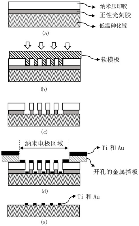
[0004] In order to overcome the shortcomings of high cost and slow speed of electron beam exposure, the present invention uses nanoimprinting instead of electron beam exposure, which reduces the processing cost and improves the processing speed. Shaped double-layer glue solves the problem of difficult metal peeling when conventional nanoimprinting is used in the lift-off process

Method used


Image

  • Manufacturing method of low-cost terahertz photoconductive antenna with nano electrode
  • Manufacturing method of low-cost terahertz photoconductive antenna with nano electrode
  • Manufacturing method of low-cost terahertz photoconductive antenna with nano electrode

Examples


Embodiment

[0027] After cleaning the gallium arsenide wafer prepared by low-temperature growth, spin-coat a layer of S1805 positive photoresist solution with a concentration of 20wt%, with a thickness of 60nm, bake it on a hot plate at 95°C for 60s, and then spin-coat a layer of nano-pressurized Printing glue, the thickness is 200nm. Use a conventional hard template to pre-print a DMS soft template with a sub-micron precision nano-electrode pattern structure, and then use the DMS soft template to perform heat-assisted UV imprinting to transfer the sub-micron precision nano-electrode pattern to the adhesive film, and then Remove soft templates. Use oxygen plasma etching technology to remove the nano-imprint glue and S1805 positive photoresist in the imprint trench, exposing the gallium arsenide wafer. Rinse with 1wt% KOH solution for 9 seconds, dissolve part of the photoresist laterally, and obtain an inverted double-layer adhesive film in the nano-electrode area, and then bake it on a h...


PUM

PropertyMeasurementUnit
thicknessaaaaaaaaaa
thicknessaaaaaaaaaa
thicknessaaaaaaaaaa

Abstract

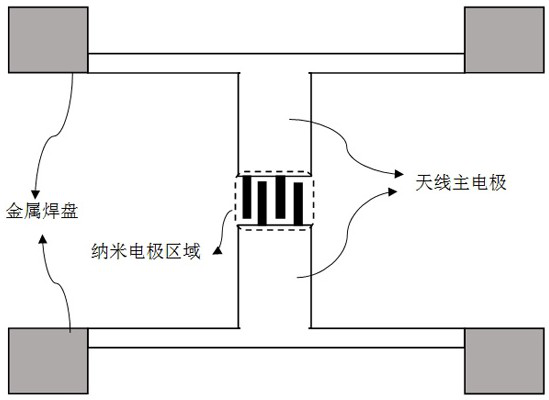
The invention discloses a method for manufacturing a low-cost terahertz photoconductive antenna with a nano electrode, which comprises the following steps of: processing inverted-table-shaped double-layer glue by combining nano imprinting and developing lateral etching, and reducing the area of a metal film by using a perforated metal baffle when a metal coating is prepared. The problem that metalstripping is difficult when a lift-off process is used for machining a nano electrode is solved. Meanwhile, a soft template which is reprinted from a hard template and can be used repeatedly is used,a nano-electrode with submicron precision is processed by a nano-imprinting technology, and a main electrode with micron precision is processed by mask photoetching, so that the processing speed of the terahertz photoconductive antenna is increased, the processing cost is reduced, and the terahertz photoconductive antenna is suitable for mass production.

Description

technical field [0001] The invention relates to the processing of terahertz devices, in particular to a method for manufacturing a terahertz photoconductive antenna with nano-electrodes capable of reducing costs and realizing mass production. Background technique [0002] Terahertz (THz) waves refer to electromagnetic wave radiation with a frequency range of 0.1-10THz, which is between infrared rays and microwaves. Compared with other bands, terahertz has low energy, coherence, rich spectrum fingerprints of matter, and is transparent to non-polar materials. Therefore, THz radiation is widely used in physics, chemistry, astronomy, security inspection, wireless communication and Medical science and other fields have great research value and application prospects. The generation of THz radiation is the key to the development and application of THz science and technology. Among the many kinds of THz sources, the use of semiconductor-based terahertz photoconductive antennas as ...

Claims


Application Information

Patent Timeline
Patent Type & Authority Applications(China)
IPC IPC(8): G03F7/00G03F7/20G03F7/42
CPCG03F7/0002G03F7/20G03F7/427
Inventor 陈景源
Owner FUJIAN Z K LITECORE LTD
Learn More