
Junction field effect transistor and preparation method thereof

A field-effect transistor and junction technology, which is applied in semiconductor/solid-state device manufacturing, semiconductor devices, electrical components, etc., can solve problems such as general stability, lack of exploration and innovation, and general device performance, so as to ensure purity and reduce sub- Threshold swing, effect of suppressing interface defects

Active Publication Date: 2021-03-05
NANJING UNIV OF SCI & TECH
View PDF2 Cites 1 Cited by
  • Summary
  • Abstract
  • Description
  • Claims
  • Application Information

AI Technical Summary

Problems solved by technology

Pyo Jin Jeon of Yonsei University used black phosphorus (BP) and ZnO materials to construct a heterojunction. Although the prepared JFET realized the inverter function of a logic circuit, its on-off current ratio was only about 10. 4 , the average subthreshold swing is greater than 300mV / dec, and the stability is average (Nano Lett., 2016, 16, 1293-1298)
The June Yeong Lim research group and others also at Yonsei University in South Korea, based on two TMDCs materials (MoTe 2 and MoS 2 ) to construct a JFET, although the obtained device has a high mobility and a subthreshold swing reduced to 204mV / dec, the maximum switching current ratio exhibited by the device is only 5×10 4 (NPJ 2D Mater. and Appl., 2018, 2, 37)
In these existing works, researchers have made some more traditional TMDC materials and metal oxide semiconductor materials into heterojunctions to further construct JFET devices, lacking exploration and innovation in material selection, and the performance of the devices average performance

Method used


Image

  • Junction field effect transistor and preparation method thereof
  • Junction field effect transistor and preparation method thereof
  • Junction field effect transistor and preparation method thereof

Examples


Embodiment

[0032] The thickness of the tungsten disulfide thin film in this embodiment is 10nm, InGeTe 3 The thickness of the film was 150 nm.

[0033] In the junction field effect transistor prepared in this embodiment, the substrate is Si / SiO 2 , the source electrode, the drain electrode and the top gate electrode are Cr / Au, the thickness of which is Cr: 10nm, Au: 50nm.

[0034] The specific preparation process is:

[0035] (1) Select a thermally oxidized silicon wafer as the substrate, first use ethanol, acetone, and deionized water to ultrasonically for 5 minutes, then heat-treat the substrate on a heating platform at 300°C for 1 hour, and store it in a dry environment;

[0036] (2) Prepare Scotch tape, put WS 2 The single crystal was repeatedly peeled and glued on Scotch tape until the surface of the tape had no obvious ups and downs, and then the tape was pasted on the surface of the silicon oxide substrate and pressed tightly. After 6 hours, the tape was removed, and the desire...


PUM

PropertyMeasurementUnit
Thicknessaaaaaaaaaa
Thicknessaaaaaaaaaa

Abstract

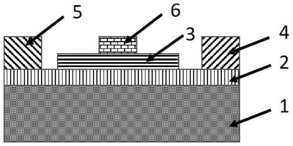
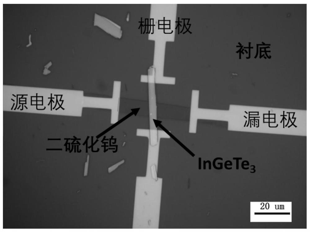
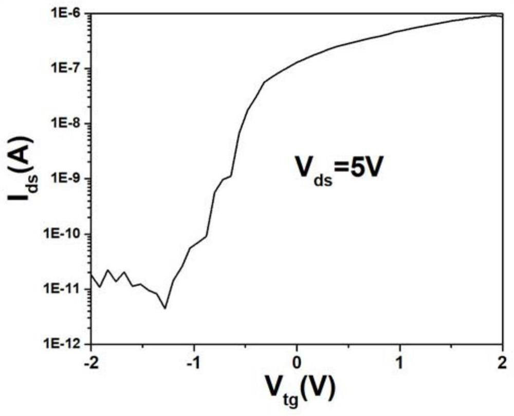
The invention discloses a junction field effect transistor and a preparation method thereof. The junction field effect transistor comprises a substrate, an N-type tungsten disulfide film, a P-type InGeTe3 film, a source electrode, a drain electrode and a top gate electrode, the N-type tungsten disulfide film is arranged on the surface of the substrate, the source electrode and the drain electrodeare arranged at the two ends of the surface of the N-type tungsten disulfide film, and the P-type InGeTe3 film is arranged on the surface of the N-type tungsten disulfide film; and the top gate electrode is arranged on the surface of the P-type InGeTe3 thin film and located between the source electrode and the drain electrode. According to the invention, WS2 and InGeTe3 are applied to the JFET, the width of a depletion region in the N-type tungsten disulfide thin film is realized by regulating and controlling the voltage of the P-type InGeTe3 thin film, the adjustment of channel conductivity is realized, the generation of interface defects is inhibited, the influence of the interface state on carrier transport is reduced, the sub-threshold swing of the device is reduced by virtue of the advantage of no complex dielectric engineering of the JFET, and the switching ratio and the current density are improved.

Description

technical field [0001] The invention belongs to the technical field of semiconductors, and relates to a junction field effect transistor and a preparation method thereof, in particular to an InGeTe-based 3 and tungsten disulfide junction field effect transistor and its preparation method. Background technique [0002] with WS 2 and MoS 2 The representative two-dimensional transition metal dichalcogenides (TMDCs) are considered to be semiconductor materials with great potential due to their atomic-level thickness, adjustable band gap, no surface dangling bonds, and superior mechanical properties. , wearable flexible devices, military information and other fields have broad application prospects. And InGeTe 3 As a new type of ternary material with layered structure, due to its excellent physical and chemical properties, it has become a new star in the field of low-dimensional material research. In theoretical prediction, InGeTe 3 Materials are direct semiconductors from ...

Claims


Application Information

Patent Timeline
IPC IPC(8): H01L29/808H01L29/267H01L21/335
CPCH01L29/8086H01L29/267H01L29/66969
Inventor 张胜利周戬程子超高洁宋秀峰陈翔
Owner NANJING UNIV OF SCI & TECH
Learn More