An organic light emitting device

A technology of organic light-emitting devices and organic substances, which is applied in the manufacture of electric solid-state devices, semiconductor devices, semiconductor/solid-state devices, etc. Luminous efficiency and driving voltage, and the effect of improving luminous efficiency

Active Publication Date: 2022-04-08
CHANGCHUN HYPERIONS TECH CO LTD
View PDF6 Cites 0 Cited by
  • Summary
  • Abstract
  • Description
  • Claims
  • Application Information

AI Technical Summary

Problems solved by technology

In a top-emitting device, the light emitted by the light-emitting layer will be reflected and refracted at the interface of other organic functional layers. The optical waveguide effect and the surface plasmon element effect of the device make most of the photons non-radiatively coupled and converted to thermal energy. The form of consumption, resulting in a huge gap between internal and external quantum efficiency, is one of the main reasons for the poor efficiency and life of the device

Method used


Image

  • An organic light emitting device
  • An organic light emitting device
  • An organic light emitting device

Examples


preparation example Construction

[0142] The preparation and formation methods of each layer in the organic light-emitting device are not particularly limited, and vacuum evaporation method, spin coating method, vapor deposition method, blade coating method, laser thermal transfer method, electrospray coating method, slit coating method can be used. Either of the cloth method and the dip coating method, the method of vacuum vapor deposition is preferably used in the present invention.

[0143] The organic light-emitting device of the present invention can be widely used in the fields of panel display, lighting source, flexible OLED, electronic paper, organic solar cell, organic photoreceptor or organic thin film transistor, signboard, signal lamp and the like.

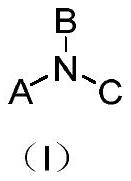
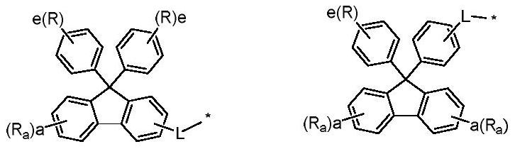
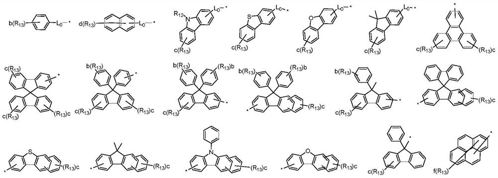
[0144] The second hole transport layer made of the material of formula (I) and the covering layer made of the material of formula (IV), the corresponding compounds can be obtained by the following methods:

[0145] The triarylamine compound represent...

Embodiment 1

[0154] [Example 1] Synthesis of Compound 1-1

[0155]

[0156] Step1: Synthesis of intermediate A-1

[0157] Under nitrogen protection, toluene (600mL), a-1 (20.00g, 0.06mol), b-1 (23.83g, 0.06mol), palladium acetate (0.21g, 0.93mmol), tert- Sodium butoxide (11.3 g, 0.117 mol) and tri-tert-butylphosphine (8 mL in toluene). And react under the condition of reflux for 2 hours. After the reaction stopped, the mixture was cooled to room temperature, filtered with diatomaceous earth, the filtrate was concentrated, recrystallized with methanol, filtered with suction and rinsed with methanol to obtain a recrystallized solid to obtain intermediate A-1 (30.41g, yield 78%) , HPLC detection solid purity ≧ 99.7%.

[0158] Step2: Synthesis of compound 1-1

[0159] Under nitrogen protection, toluene solvent (600ml), c-1 (5.83g, 36mmol), intermediate A-1 (23.39g, 36mmol), Pd 2 (dba) 3 (330mg, 0.36mmol), BINAP (0.67g, 1.08mmol) and sodium tert-butoxide (3.23g, 33.6mmol), stirred and ...

Embodiment 2

[0161] [Example 2] Synthesis of Compound 1-22

[0162] Compound 1-22 (17.66 g) was synthesized by the method of compound 1-1 above, and the purity of the solid was detected by HPLC ≧99.7%. Mass Spectrum m / z: 730.3419 (Theoretical: 730.3396). Theoretical element content (%)C 56 h 34 D. 5 N: C, 92.02; H, 6.07; N, 1.92 Measured element content (%): C, 92.02; H, 6.07; N, 1.95.


PUM

PropertyMeasurementUnit
wavelengthaaaaaaaaaa
thicknessaaaaaaaaaa
thicknessaaaaaaaaaa

Abstract

The invention provides an organic light-emitting device and relates to the technical field of organic electroluminescence. The provided organic light-emitting device includes a substrate, an anode, an organic layer, a cathode, and a cover layer, the organic layer includes a hole injection layer and a hole transport layer, and the hole transport layer includes a first hole transport layer and a second hole transport layer. hole transport layer. The organic light-emitting device prepared by the invention improves the characteristics of the device, effectively improves the luminous efficiency of the organic light-emitting device, and reduces the driving voltage of the device. The organic light-emitting device of the present invention has good application effect and industrialization prospect, and can be widely used in panel display, lighting source, flexible OLED, electronic paper, organic solar cell, organic photoreceptor or organic thin film transistor, signage, signal lamp and other fields.

Description

technical field [0001] The invention relates to the technical field of organic electroluminescence, in particular to an organic light emitting device. Background technique [0002] After nearly 30 years of development, organic light-emitting diodes (OLEDs) have achieved rich results in material development and device structure design. OLEDs have begun large-scale commercial use in displays, especially high-end smartphones. An organic light-emitting device refers to a device in which holes injected from the anode and electrons injected from the cathode are transported and recombined in the organic functional layer to form excitons, and then radiate and emit photons. In terms of display, OLED has many advantages compared with the popular liquid crystal display (LCD): (1) the thickness can be less than 1 mm, only 1 / 3 of the LCD screen, and the weight is lighter; The problem of viewing angle. Even when viewed from a large viewing angle, the picture is still not distorted; (3) ...

Claims


Application Information

Patent Timeline
Patent Type & Authority Patents(China)
IPC IPC(8): H01L51/50H01L51/54
CPCH10K85/111H10K50/156H10K50/15Y02E10/549
Inventor 朱鸫达赵璐王小会鲁秋
Owner CHANGCHUN HYPERIONS TECH CO LTD
Why Eureka
Try Eureka