Etching solution for low-resistance silicon product and etching method thereof

An etching solution and low-resistance technology, applied in chemical instruments and methods, circuits, electrical components, etc., can solve problems such as great impact on human health, large environmental pollution, and easy generation of bubbles, and achieve uniform and non-violent reactions and reduce risks. The effect of resistance and small amount of etching

Active Publication Date: 2021-04-16
CHONGQING GENORI IND CO LTD
View PDF10 Cites 0 Cited by
  • Summary
  • Abstract
  • Description
  • Claims
  • Application Information

AI Technical Summary

Problems solved by technology

The original etching solution is prepared from hydrofluoric acid, nitric acid, acetic acid and water. The use of high-concentration and highly corrosive strong acids will have a great impact on the health of the operator during the preparation process, and the toxic gas produced will affect the environment. Large pollution, and at the same time, the amount of etching is small within a certain period of time, the efficiency is low, and the reaction is violent and easy to generate bubbles

Method used


Image

  • Etching solution for low-resistance silicon product and etching method thereof
  • Etching solution for low-resistance silicon product and etching method thereof
  • Etching solution for low-resistance silicon product and etching method thereof

Examples


Embodiment 1

[0035] An etchant for low-resistance silicon products, by mass percentage, consists of the following substances:

[0036]

[0037] Solution preparation method: Weigh the required ammonium bifluoride according to the proportion, add an appropriate amount of water to dissolve, then slowly add potassium nitrate, phosphoric acid, sulfuric acid and ammonium persulfate according to the amount, stir evenly, cool to room temperature, and add octylphenol Polyoxyethylene ether and polyethylene glycol, plus the balance of water to volume. It is preferable to use ultrapure water of 18MΩ.cm.

[0038] Etching method: heat the solution to 30°C, put the product into the solution, rotate at a constant speed, the etching time is 3 minutes, and the double-sided etching amount can reach 0.04mm. If you need to increase the amount of etching, you can increase the solution temperature or extend the etching time to achieve the effect. The temperature of the solution cannot be higher than 40°C, o...

Embodiment 2

[0047] An etchant for low-resistance silicon products, by mass percentage, consists of the following substances:

[0048]

[0049] Solution preparation method and etching method are the same as embodiment 1.

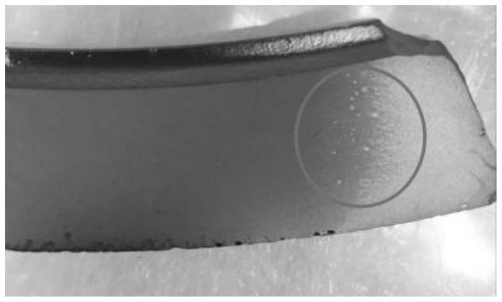
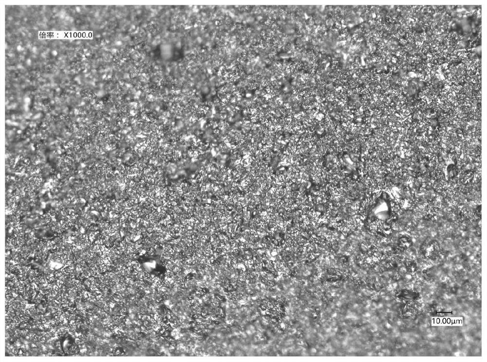
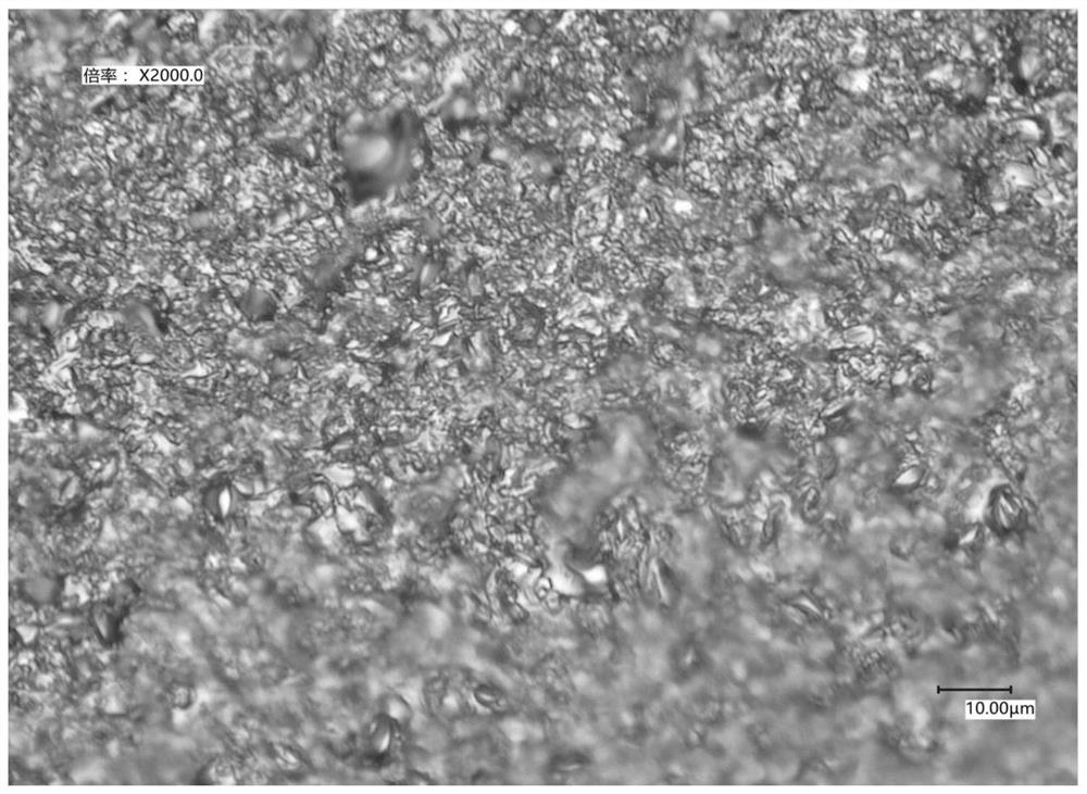
[0050] Figure 7 This is the partial appearance of the sample after etching in this embodiment, the surface is fine and uniform, without color difference or bubble holes.

Embodiment 3

[0052] An etchant for low-resistance silicon products, by mass percentage, consists of the following substances:

[0053]

[0054]

[0055] Solution preparation method and etching method are the same as embodiment 1.

[0056] Figure 8 This is the partial appearance of the sample after etching in this embodiment, the surface is fine and uniform, without color difference or bubble holes.


PUM

PropertyMeasurementUnit
electrical resistivityaaaaaaaaaa

Abstract

The invention relates to an etching solution for a low-resistance silicon product. The etching solution is composed of an aqueous solution of ammonium bifluoride, potassium nitrate, sulfuric acid, ammonium persulfate, octylphenol polyoxyethylene ether, polyethylene glycol and phosphoric acid. When ammonium bifluoride and sulfuric acid are properly proportioned, a certain amount of HF can be generated according to a certain rate, and a small amount of potassium nitrate, ammonium persulfate and phosphoric acid are proportioned and then etched. Incomplete or non-uniform etching caused by incomplete contact between the etching liquid and the surface of the silicon product due to a large number of bubbles generated in the reaction process is reduced, and spots are reduced. The etching solution uniformly etches the surface of the product, ions in the solution are quickly and uniformly dispersed during reaction, and the surface of the product does not generate a non-uniform chromatic aberration phenomenon. The reaction is uniform and not violent, the etching rate is uniform, and the roughness is almost the same as that before etching.

Description

technical field [0001] The invention belongs to the technical field of semiconductor preparation, and relates to an etching solution for low-resistance silicon products and an etching method thereof. Background technique [0002] Semiconductors now account for a large portion of the world economy and have a huge influence on economic growth. Semiconductor technology is developing at an ever-changing speed. Now the 12-inch wafer semiconductor production process is produced in China, and China is the largest semiconductor consumer in the world no matter compared with any semiconductor manufacturing country in the world. [0003] However, with the development of semiconductor technology, the ever-expanding wafers also begin to require highly integrated and high-precision circuits. In the semiconductor slicing production process using silicon wafers as raw materials, equipment accessories that affect circuit integration need to be used with wafers. The raw material is the same ...

Claims


Application Information

Patent Timeline
Patent Type & Authority Applications(China)
IPC IPC(8): C09K13/08H01L21/306
Inventor 王燕清
Owner CHONGQING GENORI IND CO LTD
Why Eureka
Try Eureka