Carbon dioxide sensor for monitoring microbial growth and preparation method thereof

A carbon dioxide, sensor technology, applied in instruments, scientific instruments, measuring devices, etc., can solve the problems of low utilization, limited use, large volume, etc.

Pending Publication Date: 2021-04-30
TAIYUAN UNIV OF TECH
View PDF0 Cites 2 Cited by
  • Summary
  • Abstract
  • Description
  • Claims
  • Application Information

AI Technical Summary

Problems solved by technology

Therefore, the gas concentration can be measured by measuring the attenuation of infrared light by the gas, but the carbon dioxide sensor prepared based on this technol

Method used


Image

  • Carbon dioxide sensor for monitoring microbial growth and preparation method thereof
  • Carbon dioxide sensor for monitoring microbial growth and preparation method thereof
  • Carbon dioxide sensor for monitoring microbial growth and preparation method thereof

Examples


preparation example Construction

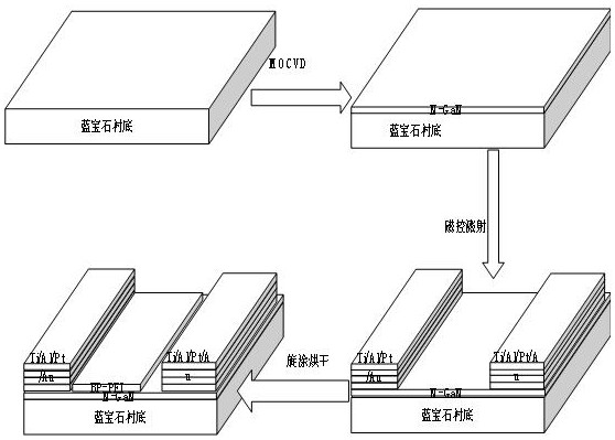
[0040] A preparation method for a carbon dioxide sensor for monitoring microbial growth, comprising the steps of:

[0041] Step 1: epitaxially grow silicon-doped n-type gallium nitride epitaxial wafers on a sapphire substrate;

[0042] Step 2: Deposit a SiO2 layer on the surface of the n-type gallium nitride epitaxial wafer by PECVD method, place a mask after removing the photoresist, and prepare an in-situ mask by using exposure and development processes;

[0043] Using magnetron sputtering technology to deposit Ti / Al / Pt / Au electrodes on the surface of n-type GaN epitaxial wafers to form ohmic contact with GaN epitaxial wafers;

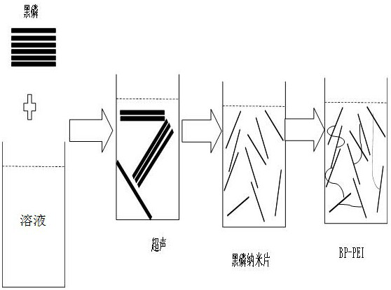
[0044] Step 3: Using single crystal black phosphorus as a raw material, use a simple liquid phase exfoliation method to peel it into two-dimensional thin-layer black phosphorus single layer and multi-layer micro-nano sheets with a thickness of 1-20 nm;

[0045] The ultrasonic energy generated by the cell ultrasonic breaker is used to peel off the si...

Embodiment 1

[0075] S1: A silicon-doped n-GaN epitaxial wafer was epitaxially grown on a four-inch sapphire substrate by metal-organic chemical vapor deposition (MOCVD). The thickness of the gallium nitride layer was 35 nm, and the silicon doping concentration was 1×10 18 cm -3 -9×10 18 cm -3 .

[0076] S2: Depositing 30nm SiO on the surface of GaN epiwafer by PECVD 2 After removing the photoresist, place a mask plate, use a series of processes such as exposure and development to prepare an in-situ mask plate, and use magnetron sputtering technology to deposit Ti / Al / Pt / Au electrodes on GaN epitaxial wafers, so that It forms an ohmic contact with the GaN epiwafer for good electrical performance. Afterwards, split the GaN epitaxial wafers on which the electrodes have been prepared, so that the four-inch GaN epitaxial wafers are evenly divided into 5 mm×5 mm epitaxial wafers.

[0077] S3: Using single crystal black phosphorus as raw material, it is exfoliated into a 1-20 nm thick two-dim...

Embodiment 2

[0082] S1: An n-type gallium nitride layer was epitaxially grown on a sapphire substrate by metal-organic chemical vapor deposition. The thickness of the gallium nitride layer was 35 nm, and the silicon doping concentration was 1×10 18 cm −3 - 9×10 18 cm −3 .

[0083] S2: Depositing 30nm SiO on the surface of GaN epiwafer by PECVD 2 Layer, place the mask plate after throwing the photoresist, exposure, development and other processes to prepare the in-situ mask plate, and use the magnetron sputtering technology to deposit Ti / Al / Pt / Au electrodes on the gallium nitride epitaxial wafer to make it Form ohmic contact with GaN epiwafer for good electrical performance. Afterwards, split the GaN epitaxial wafers on which the electrodes have been prepared, so that the four-inch GaN epitaxial wafers are evenly divided into 5 mm×5 mm epitaxial wafers.

[0084] S3: Exfoliate the black phosphorus flakes from the bulk black phosphorus in the liquid phase, first use a mortar to grind the...


PUM

PropertyMeasurementUnit
Thicknessaaaaaaaaaa
Thicknessaaaaaaaaaa
Thicknessaaaaaaaaaa

Abstract

The invention discloses a carbon dioxide sensor for monitoring microbial growth and a preparation method thereof, and belongs to the technical field of carbon dioxide sensors and preparation methods thereof. The technical problem to be solved is to provide an improvement of a carbon dioxide sensor hardware structure for monitoring microbial growth. According to the technical scheme, an n-type gallium nitride layer is grown on a sapphire substrate in an epitaxial mode, a Ti/Al/Pt/Au electrode is deposited on a gallium nitride epitaxial wafer through a series of electrode preparation processes, and then a BP-PEI layer is prepared through liquid phase stripping of black phosphorus and functional modification of the black phosphorus, so that the miniaturized carbon dioxide gas sensor which is high in sensitivity and can be operated in real time is obtained. The carbon dioxide sensor is stable in performance, good in carbon dioxide gas-sensitive performance, low in price, small in size and simple in detection mode, and has the advantages of being disposable, free of pollution and the like. The carbon dioxide sensor is applied to monitoring of microbial growth.

Description

technical field [0001] The invention discloses a carbon dioxide sensor for monitoring microbial growth and a preparation method thereof, belonging to the technical field of carbon dioxide sensors and preparation methods thereof. Background technique [0002] During the growth process of microorganisms, they constantly exchange materials and energy with the outside world, and the growth process can be monitored through the pH of the microbial incubator, oxygen consumption rate, and carbon dioxide content. The biological incubator is a long-term sealed device. The composition and gas concentration of the medium will change relative to the initial state. Under different gas environments, the growth rate and metabolites of microorganisms will change accordingly. Today, the demand for monitoring microbial growth curves is very common. In order to monitor the growth of microorganisms, frequent detection of gas components is required. Similarly, detecting the concentration of carbo...

Claims


Application Information

Patent Timeline
IPC IPC(8): G01N27/12
CPCG01N27/12G01N27/127G01N27/126
Inventor 韩丹韩晓美桑胜波禚凯冀健龙张文栋
Owner TAIYUAN UNIV OF TECH
Why Eureka
Try Eureka