Preparation method and application of nanostar chain-shaped nanostructure arrays

A technology of nanostructure and micro-nanostructure, applied in the direction of nanotechnology, nanotechnology, nanotechnology for materials and surface science, etc., can solve the problem of limited improvement

Pending Publication Date: 2021-05-11
JIANGSU UNIV OF TECH
View PDF7 Cites 2 Cited by
  • Summary
  • Abstract
  • Description
  • Claims
  • Application Information

AI Technical Summary

Problems solved by technology

Although the discrete point array can improve the local field enhancement effect to a certain extent, the degree of improvement is limited.

Method used


Image

  • Preparation method and application of nanostar chain-shaped nanostructure arrays
  • Preparation method and application of nanostar chain-shaped nanostructure arrays
  • Preparation method and application of nanostar chain-shaped nanostructure arrays

Examples


Embodiment 1

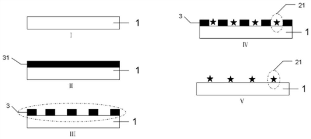
[0033] A photoresist layer with a two-dimensional strip-shaped hollow unit structure is prepared by wet etching, and the process is as follows figure 2 Shown:

[0034] First substrate 1, such as glass or conductive glass or silicon wafer, is thoroughly cleaned by detergents such as acetone, isopropanol, etc., to remove impurity ions (such as Figure 2-I );

[0035] Then spin-coat one layer of positive photoresist film 31 (such as Figure 2-Ⅱ ), the thickness of the photoresist layer is more than 200nm, after drying, the mask plate with the two-dimensional strip micro-nano structure array pattern is used for exposure, after the exposure, post-baking and development are carried out, so that the surface of the substrate 1 is obtained. The photoresist layer 3 of the micro-nano structure array pattern (such as figure 2 -III), the micro-nano structure array pattern is composed of a plurality of two-dimensional strip-shaped hollow unit structures, and the process of exposure and...

Embodiment 2

[0039] Preparation of gold nanostar particle sol:

[0040] ① Mix 0.250mL chloroauric acid solution (0.01M) and 7.5mL CTAB solution (0.1M) evenly, add 0.6mL sodium borohydride solution (0.01M), and shake gently to form a dark brown gold seed solution, which Store in the dark for 2 hours before use;

[0041] ② Take another 10mL vial, add 4.75mL of the above CTAB solution and 0.2mL of the above chloroauric acid solution into the vial, shake gently to mix the two evenly, then add 0.03mL of silver nitrate solution (0.01M) and 0.032mL of Ascorbic acid solution (0.1M), after mixing, a colorless growth solution is obtained, which is ready for use;

[0042] ③Then add 20μl of gold seed solution to 20mL of growth solution, shake and mix evenly, and let it stand at room temperature for more than 3 hours to obtain a dark blue gold nanostar particle sol, and then after aging for 12 hours, perform two centrifuges to remove excess reaction The pure gold nanostar particle sol was obtained. ...

Embodiment 3

[0045] Depositing Gold Nanostar Particles:

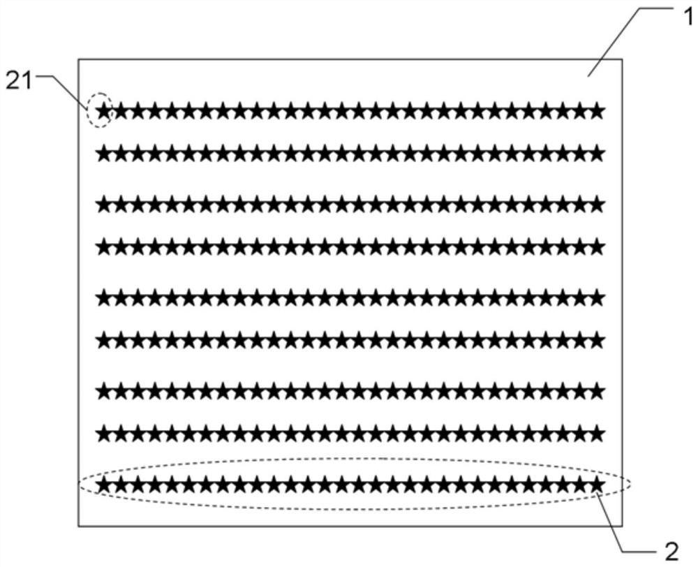
[0046] The gold nanostar particle sol (such as figure 2 -Ⅳ), and air-dried naturally, the distribution density of gold nanostars was monitored by scanning electron microscopy to ensure the formation of chain-like nanostructures of nanostars in the hollow unit structure. According to the actual situation, the sol of gold nanostar particles can be drip-coated multiple times to ensure that the gold nanostar particles are in a continuous chain distribution state in the strip-shaped hollow unit structure of the photoresist layer (such as figure 1 shown in Mark 2).


PUM

PropertyMeasurementUnit
thicknessaaaaaaaaaa
widthaaaaaaaaaa
sizeaaaaaaaaaa

Abstract

The invention relates to a preparation method and application of nanostar chain-shaped nanostructure arrays, The preparation method comprises the following steps: (1) wet etching is carried out on the surface of a substrate material to obtain a photoresist layer with a micro-nano structure array pattern, and the micro-nano structure array pattern is composed of a plurality of two-dimensional strip-shaped hollow unit structures; and (2) nano-star particle sol is repeatedly dispensed on the surface of the substrate material with the photoresist layer and naturally dried, gold nano-star particles are deposited in the hollow unit structures, and finally the multiple nano-star chain-shaped nano-structure arrays are obtained on the surface of the substrate material after the photoresist is removed. According to the preparation method, discrete nano-materials in the prior art can be constructed into nano-chains with nanoscale, so that the distance between nano-particles reaches nanoscale, the distance between nano-chains also has nanoscale, the nano-chains can be applied to a surface-enhanced Raman scattering substrate, the local field enhancement effect is improved, and the gold nanostar chain-shaped nanostructure arrays have a better photoelectric effect.

Description

technical field [0001] The invention relates to the field of nanomaterial preparation, in particular to a preparation method and application of a nanostar chain nanostructure array. Background technique [0002] In recent years, noble metal nanomaterials have aroused widespread interest in the field of nanotechnology due to their unique optical, electrical, mechanical, catalytic, and biocompatibility properties, especially in photovoltaic enhancement or Raman inspection technology. prospect. [0003] The surface plasmon effect of metal nanoparticles is due to the fact that the electron cloud on the surface of the nanoparticle is excited by the electric field in the incident electromagnetic wave (or incident light), and interacts to form surface plasmons. Such surface plasmons can generate electric fields with magnitudes higher than that of incident electromagnetic waves by 10 3 -10 7 times the local electric field strength. In nanotechnology, it's called a hotspot. In t...

Claims


Application Information

Patent Timeline
Patent Type & Authority Applications(China)
IPC IPC(8): B22F9/24B22F1/00B82Y30/00B82Y40/00G01N21/65
CPCB22F9/24G01N21/658B82Y30/00B82Y40/00B22F1/0553B22F1/054
Inventor 朱圣清向萌张洪硕周鹏
Owner JIANGSU UNIV OF TECH
Why Eureka
Try Eureka