Structure for improving breakdown voltage of gallium nitride HEMT power device and preparation method thereof

A power device and breakdown voltage technology, applied in semiconductor/solid-state device manufacturing, semiconductor devices, circuits, etc., can solve the problems of reducing device frequency characteristics, gate leakage current, gate leakage, etc., to achieve high drain voltage, The effect of increasing breakdown voltage without degrading frequency characteristics

Inactive Publication Date: 2021-06-01
NO 55 INST CHINA ELECTRONIC SCI & TECHNOLOGYGROUP CO LTD
View PDF0 Cites 2 Cited by
  • Summary
  • Abstract
  • Description
  • Claims
  • Application Information

AI Technical Summary

Problems solved by technology

When the electric field strength exceeds the withstand voltage capability of the device, the device is prone to breakdown
[0005] 2. Gate leakage current; surface defects, contamination, dangling bonds, etc. of the device are easy to form a surface state, and the surface drift point to the phenomenon causes the leakage current of the gate
However, the introduction of field plates will bring additional capacitance and reduce the frequency characteristics of the device

Method used


Image

  • Structure for improving breakdown voltage of gallium nitride HEMT power device and preparation method thereof
  • Structure for improving breakdown voltage of gallium nitride HEMT power device and preparation method thereof
  • Structure for improving breakdown voltage of gallium nitride HEMT power device and preparation method thereof

Examples


Embodiment 1

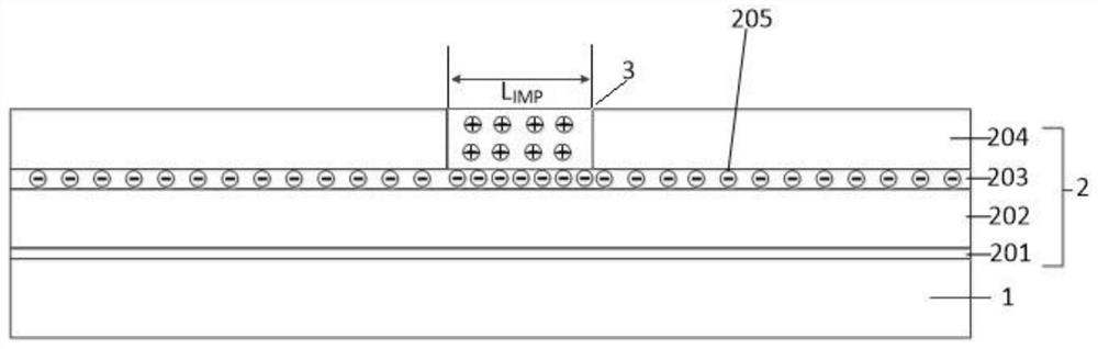
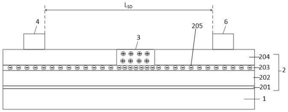
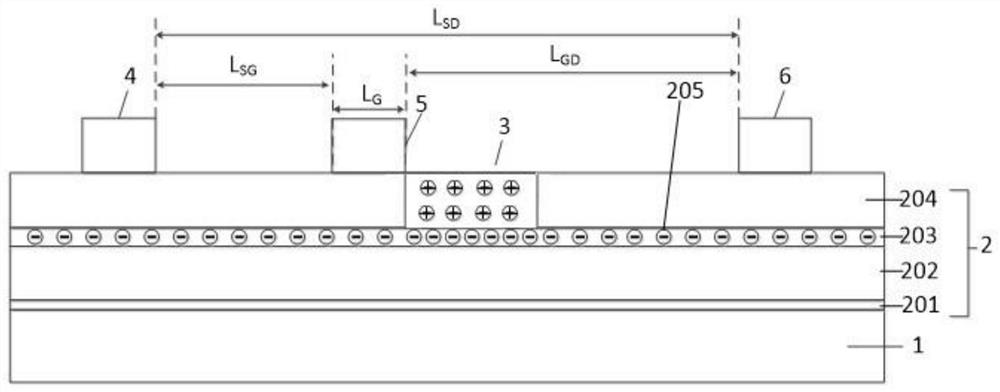
[0036] refer to Figure 1A-Figure 1C , a method for preparing a structure for improving the breakdown voltage of a gallium nitride HEMT power device in this embodiment, comprising the following steps:

[0037] Step 1: If Figure 1A As shown, silicon carbide is selected as the material of the substrate 1, and the nucleation layer 201, the first material layer 202, the channel layer 203 and the second material layer 204 are sequentially formed on the substrate 1 from bottom to top; wherein the nucleation layer 201 The material is aluminum nitride, the material of the first material layer 202 is gallium nitride, the material of the channel layer 203 is gallium nitride, and the material of the second material layer 204 is aluminum gallium nitride; The dopant region is shielded, and the implantation process is used to introduce arsenic ions into the second material layer 204 with a concentration of 5×10 13 cm -3 , form the ion-doped region 3, the width of the ion-doped region 3 ...

Embodiment 2

[0043] refer to Figure 2A-Figure 2C , a method for preparing a structure for improving the breakdown voltage of a gallium nitride HEMT power device in this embodiment, comprising the following steps:

[0044] Step 1: If Figure 2A As shown, silicon carbide is selected as the material of the substrate 1, and the nucleation layer 201, the first material layer 202, the channel layer 203, the third material layer 206 and the second material layer 204 are sequentially formed on the substrate 1 from bottom to top; The material of the nucleation layer 201 is aluminum nitride, the material of the first material layer 202 is gallium nitride, the material of the channel layer 203 is gallium nitride, the material of the third material layer 206 is indium gallium nitride, and the material of the second material layer 202 is gallium nitride. The material of layer 204 is aluminum gallium nitride; the non-ion-doped region is blocked by photolithography process, and fluorine ions are introd...

Embodiment 3

[0050] refer to Figure 3A-Figure 3C , a method for preparing a structure for improving the breakdown voltage of a gallium nitride HEMT power device in this embodiment, comprising the following steps:

[0051] Step 1: If Figure 3A As shown, silicon carbide is selected as the material of the substrate 1, and the nucleation layer 201, the first material layer 202, the channel layer 203, the second material layer 204, and the fourth material layer 207 are sequentially formed on the substrate 1 from bottom to top; The material of the nucleation layer 201 is aluminum nitride, the material of the first material layer 202 is gallium nitride, the material of the channel layer 203 is gallium nitride, the material of the second material layer 204 is aluminum gallium nitride, the fourth material The material of layer 207 is gallium nitride; the non-ion-doped region is blocked by photolithography process, and phosphorus ions are introduced into the second material layer 204 and the four...


PUM

PropertyMeasurementUnit
breakdown voltageaaaaaaaaaa

Abstract

The invention provides a structure for improving the breakdown voltage of a gallium nitride HEMT power device and a preparation method of the structure. The structure comprises a substrate, an epitaxial layer, a source electrode, a drain electrode and a grid electrode. The epitaxial layer is arranged above the substrate and comprises a nucleating layer, a first material layer, a channel layer and a barrier layer which are arranged from bottom to top; the channel layer is internally provided with two-dimensional electron gas, and the barrier layer is internally provided with an ion doped region. The ion doping region is introduced between the grid electrode and the drain electrode, the two-dimensional electron gas concentration of partial region in the channel is changed, the electric field distribution is changed on one side of the grid electrode, the peak electric field is obviously lower than that of a device without the ion doping region, the electric field uniformity between the grid electrode and the drain electrode is enhanced, and the electric field distribution is effectively improved; and advanced breakdown of the device caused by a grid edge electric field peak value is avoided, and the device can bear higher drain voltage. And finally, the breakdown voltage of the device is improved, and the frequency characteristic of the device is not reduced.

Description

technical field [0001] The invention belongs to the technical field of power semiconductors, and in particular relates to a structure for improving the breakdown voltage of gallium nitride HEMT power devices and a preparation method thereof. Background technique [0002] As the third-generation wide bandgap compound semiconductor material, GaN has the characteristics of large bandgap, high breakdown voltage, fast electron drift and strong radiation resistance. HEMT devices with AlGaN / GaN structure have high temperature resistance, high voltage resistance, good High frequency and high power characteristics. The AlGaN / GaN heterojunction has a strong polarization effect, even when undoped, the device can obtain up to 1×10 13 cm -2 Two-dimensional electron gas with areal density. In recent years, on the basis of the existing AlGaN / GaN heterostructure, how to further optimize the GaN HEMT device structure and improve the device breakdown voltage has become a research hotspot. ...

Claims


Application Information

Patent Timeline
Patent Type & Authority Applications(China)
IPC IPC(8): H01L29/06H01L29/778H01L21/335
CPCH01L29/0615H01L29/0623H01L29/0684H01L29/66462H01L29/7787
Inventor 邵国键林罡陈韬刘柱陈堂胜
Owner NO 55 INST CHINA ELECTRONIC SCI & TECHNOLOGYGROUP CO LTD
Why Eureka
Try Eureka