A kind of fast thermal response super black material and preparation method thereof

An ultra-black material and fast heating technology, which is applied in the metal material coating process, superimposed layer coating, vacuum evaporation coating, etc., can solve the problems such as no ultra-black coating materials, and achieve the guarantee of spectral absorption and Effect of emission, high absorption rate

Active Publication Date: 2022-08-02
UNIV OF SCI & TECH BEIJING
View PDF3 Cites 0 Cited by
  • Summary
  • Abstract
  • Description
  • Claims
  • Application Information

AI Technical Summary

Problems solved by technology

In the published literature and patents at home and abroad, although there are a large number of research reports on oriented carbon nanotubes and CVD diamond films, there is no use of microwave plasma chemical vapor deposition to directly synthesize oriented carbon nanotubes on the surface of high thermal conductivity CVD diamond films. Technical scheme of carbon nanotube ultra-black coating material

Method used


Image

  • A kind of fast thermal response super black material and preparation method thereof
  • A kind of fast thermal response super black material and preparation method thereof
  • A kind of fast thermal response super black material and preparation method thereof

Examples


Embodiment 1

[0029] 1. Select a polished single-crystal Si substrate with a size of 10 × 10 (mm), use diamond powder grinding to assist alcohol cleaning to process the sample, and then dry it and put it into a chemical vapor deposition system;

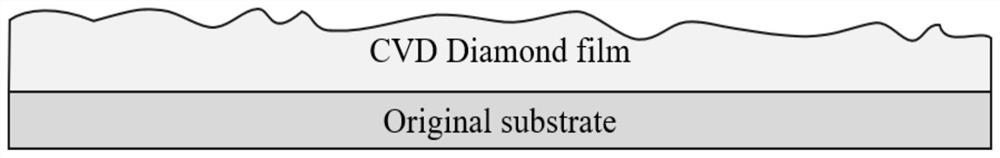
[0030] 2. A microwave plasma CVD system is used to coat a diamond film on the surface of the above-mentioned silicon wafer. A typical deposition process is: working gas hydrogen / methane, power 2.8-3.0kW, substrate temperature 800°C, methane concentration 3%, and deposition time 100h. The actual deposition thickness is about 260-280μm;

[0031] 3. Grinding and polishing the diamond film with a substrate, the surface roughness Ra of the diamond film reaches 50nm, and the film thickness is approximately 200±20μm;

[0032] 4. The "silicon / diamond" structure in step 3 is treated in 80% HF acid to remove the silicon wafer substrate.

[0033] 5. Using radio frequency magnetron sputtering technology, a layer of catalytic metal layer is formed by sputteri...

Embodiment 2

[0037] 1. Select a graphite substrate with a diameter of φ100mm, use diamond powder grinding to assist alcohol cleaning to process the sample, and then dry it and put it into a chemical vapor deposition system;

[0038] 2. Using a DC jet CVD system to prepare a diamond film on the surface of the substrate. A typical deposition process is: working gas hydrogen / methane, power of about 22kW, substrate temperature of about 900°C, methane concentration of 10%, and deposition time of 180h. The actual deposition thickness is about 1.5mm;

[0039] 3. Grinding and polishing the diamond film with substrate, the surface roughness Ra of the diamond film reaches 20-100nm, and the film thickness is 1200±100μm;

[0040] 4. Using radio frequency magnetron sputtering technology, a layer of catalytic metal layer is formed by sputtering deposition on the surface of the diamond film that has been ground and polished in step 3. The target material is a 99.99% Ni target with a vacuum degree of 5×...

Embodiment 3

[0044] 1. Select a graphite substrate with a diameter of φ100mm, use diamond powder grinding to assist alcohol cleaning to process the sample, and then dry it and put it into a chemical vapor deposition system;

[0045] 2. A diamond film is prepared on the surface of the above-mentioned substrate by DC spray CVD technology. A typical deposition process is: working gas hydrogen / methane, power of about 22kW, substrate temperature of about 900°C, methane concentration of 10%, and deposition time of 180h. The actual deposition thickness is about 1.5mm;

[0046] 3. Grinding and polishing the diamond film with substrate, the surface roughness Ra of the diamond film reaches 20-100nm, and the film thickness is 1200±100μm;

[0047] 4. Using radio frequency magnetron sputtering technology, a layer of catalytic metal layer is formed by sputtering deposition on the surface of the diamond film that has been ground and polished in step 3. The target material is Fe target with a purity of ...


PUM

PropertyMeasurementUnit
thicknessaaaaaaaaaa
surface smoothnessaaaaaaaaaa
thicknessaaaaaaaaaa

Abstract

The invention relates to a preparation method of an ultra-black material with high thermal conductivity, belonging to the field of functional materials and device manufacturing. The diamond film is deposited on the original carrier by CVD, and then the grinding, polishing and other processing procedures are completed in turn; then the catalytic metal layer is deposited on the surface of the CVD diamond film by sputtering, and the preparation of nano-catalytic particles is realized by the plasma etching and heat treatment process; Finally, carbon nanotube arrays are prepared on the surface of the diamond film to obtain a diamond / carbon nanotube ultra-black material whose size and light absorptivity meet the requirements. The element of the invention is based on diamond as a carrier, and has the characteristics of stable chemical properties, high thermal conductivity, strong light absorption and the like. In the intermediate process, physical vapor deposition coating and surface hydrogen plasma etching treatment are used to solve the problems of low density and poor orientation of carbon nanotube arrays on diamond substrates, and realize high stability and high performance all carbon-based composite functional materials. preparation. While ensuring relatively low cost, product quality and production efficiency are guaranteed.

Description

technical field [0001] The invention belongs to the field of functional material and device manufacturing, and in particular relates to a method for manufacturing an ultra-black material. Background technique [0002] Ultra-black materials have a strong ability to eliminate stray light, and are mostly used in optical systems to improve the sensitivity of optical components. For example, in the fields of space infrared camera imaging, blackbody calibration, thermoelectric power generation, and precision instruments. Even in the field of visual arts, ultra-black materials have important application prospects. Moreover, with the continuous development of functional devices in the direction of high precision and high performance, on the one hand, it is required that the absorbance of the corresponding ultra-black coating material needs to be further improved, and the spectral response band should be expanded to a broad band, so as to achieve the ability to respond to ultraviole...

Claims


Application Information

Patent Timeline
Patent Type & Authority Patents(China)
IPC IPC(8): C23C16/27C23C16/511C23C14/02C23C14/18C23C14/35C23C16/02C23C16/06C23C16/26C23C28/00
CPCC23C16/274C23C14/028C23C14/35C23C14/185C23C16/511C23C16/06C23C16/0245C23C16/26C23C16/272C23C28/322C23C28/343
Inventor 魏俊俊史佳东涂军磊李成明刘金龙陈良贤高旭辉
Owner UNIV OF SCI & TECH BEIJING
Why Eureka
Try Eureka