Charged particle beam equipment
A charged particle beam and charged particle technology, applied in the direction of circuits, discharge tubes, electrical components, etc., can solve the problems of affecting the resolution of the microscope, sample damage, and increasing the aberration of the electron beam system, so as to improve the resolution and reduce the The effect of interaction and elimination of chromatic aberration
- Summary
- Abstract
- Description
- Claims
- Application Information
AI Technical Summary
Problems solved by technology
Method used
Image
Examples
Embodiment 1
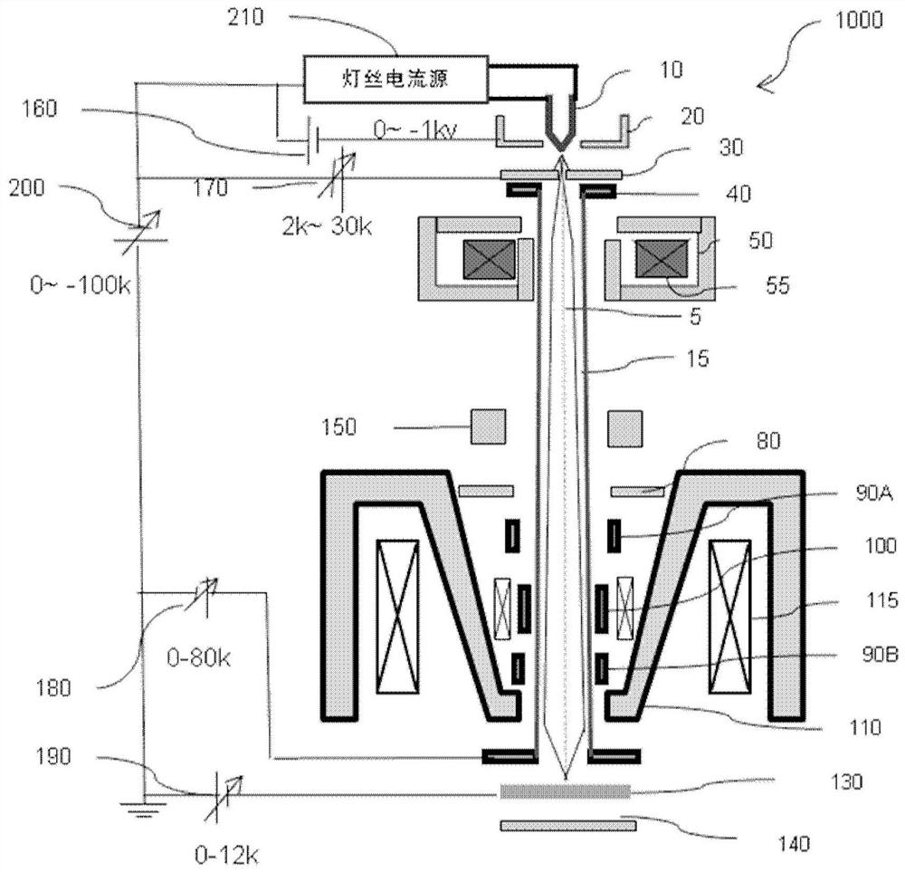
[0043] figure 1 is a schematic structural diagram of the charged particle beam device 1000 in the embodiment of the present invention. It can generate, focus, deflect and scan a charged particle beam to act on conductive or non-conductive samples.
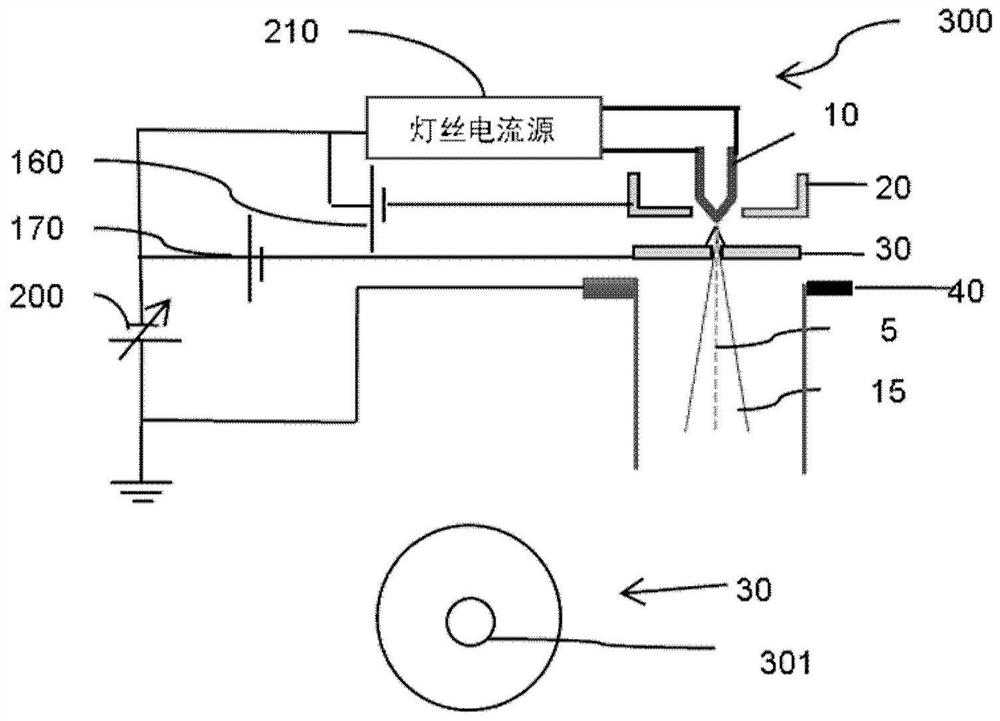
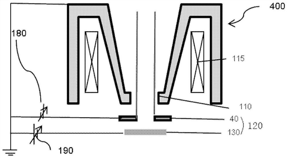
[0044] Such as Figure 1-3 As shown, the charged particle beam device includes a charged particle source 300 , a focusing magnetic mirror group, an astigmatism compensation system 150 , a scanning deflector 90 , and a composite lens group 400 .
[0045] Charged particle source 300 (see figure 1 with figure 2 ) can be a metal oxide / tungsten thermal field emission charged particle source, including a cathode 10 for generating a primary charged particle beam 15 . It also includes a Schottky electrode 20 and an extraction pole 30, which are used to generate a high-voltage electric field to absorb and accelerate the primary charged particle beam 15 emitted by the cathode 10, and then the primary charged particle beam 15 enters the ...
Embodiment 2
[0056] Such as Figure 4 As shown, the charged particle beam device in this embodiment is used as a scanning electron microscope, which can generate, focus, deflect and scan a charged particle beam to act on a conductive sample or a non-conductive sample, and collect the released charged particles or X-ray is used to generate surface topography images of samples.
[0057] On the basis of the charged particle beam apparatus in Embodiment 1, the scanning electron microscope of the present invention includes a first detection device 80 and a Wien Filter 100 .
[0058] The first detection device 80 is located above the sample 130 , and collects backscattered electrons or secondary electron signals from above the sample 130 to analyze the shape, material, conductivity and other related information of the sample. In one embodiment, the first detector 80 may be a circular scintillator detector.
[0059] The Wien filter 100 is used to screen the primary charged particle beam and the...
Embodiment 3
[0062] Such as Figure 5 As shown, the charged particle beam apparatus in this embodiment is used as a transmission electron microscope, and on the basis of the charged particle beam apparatus in Embodiment 1, the scanning electron microscope of the present invention includes a second detection device 140 .
[0063] The second detection device 140 is located below the sample 130 , and analyzes the shape, material, density and other related information of the sample surface through the transmitted charged particle signal or X-ray signal collected from the sample 130 . In one embodiment, the second detector 140 is a semiconductor direct detector, which has the characteristics of high efficiency, high speed and good signal-to-noise ratio.
[0064] Similar to Embodiment 1, the charged particles can have a landing energy of 0.1 kev to 100 kev, and in the case of low landing energy, a relatively high speed is still maintained during the journey of the charged particles, which greatl...
PUM
 Abstract
Description
Claims
Application Information
 - Generate Ideas
- Intellectual Property
- Life Sciences
- Materials
- Tech Scout
- Unparalleled Data Quality
- Higher Quality Content
- 60% Fewer Hallucinations
Browse by: Latest US Patents, China's latest patents, Technical Efficacy Thesaurus, Application Domain, Technology Topic, Popular Technical Reports.
© 2025 PatSnap. All rights reserved.Legal|Privacy policy|Modern Slavery Act Transparency Statement|Sitemap|About US| Contact US: help@patsnap.com


