
Bi (Fe, Zn) O3/NiO all-oxide thin film heterojunction used for high-speed photoelectric detection

An oxide thin film and heterojunction technology, applied in photovoltaic power generation, sustainable manufacturing/processing, circuits, etc., can solve the problem of high photogenerated electron-hole recombination rate, photoelectric response speed needs to be improved, unfavorable visible light absorption and conversion, etc. problems, achieve high-speed photoelectric response characteristics, improve carrier transport efficiency, and achieve low production costs

Active Publication Date: 2021-06-29
QINGDAO UNIV OF SCI & TECH
View PDF2 Cites 1 Cited by
  • Summary
  • Abstract
  • Description
  • Claims
  • Application Information

AI Technical Summary

Problems solved by technology

[0003] In order to further improve the photodetection performance of BFO in the visible light range, two bottlenecks must be solved: ①BFO’s band gap is too large, which is not conducive to the absorption and conversion of visible light; ②BFO is easy to form oxygen vacancies and the variable valence state of iron ions ( From Fe 3+ to Fe 2+ ), leading to a higher recombination rate of photogenerated electrons-holes, thus restricting the response speed
It can be seen that the photoelectric response speed of the above devices still needs to be improved; the charge transport layer of nanomaterials or organic materials coupled with BFO will reduce the structural stability and is not conducive to subsequent device integration
[0006] In summary, there is no research on heterojunction photodetection devices constructed by combining Zn-doped BFO and inorganic oxide charge transport materials.

Method used


Image

  • Bi (Fe, Zn) O3/NiO all-oxide thin film heterojunction used for high-speed photoelectric detection
  • Bi (Fe, Zn) O3/NiO all-oxide thin film heterojunction used for high-speed photoelectric detection
  • Bi (Fe, Zn) O3/NiO all-oxide thin film heterojunction used for high-speed photoelectric detection

Examples


Embodiment 1

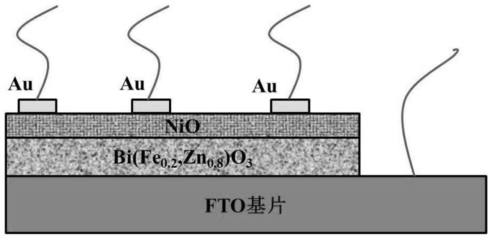
[0044] Such as figure 1 As shown, a Bi(Fe 0.2 ,Zn 0.8 )O 3 / NiO thin film heterojunction, including Bi(Fe 0.2 ,Zn 0.8 )O 3 and NiO bilayer films.

[0045] The specific process of preparing the heterojunction in this example is as follows:

[0046] Weigh iron nitrate, bismuth nitrate, and zinc nitrate powders according to the molar ratio, put them in a beaker, add 6ml of ethylene glycol methyl ether, and stir evenly at room temperature for 30 minutes. The temperature of the solution was raised to 60°C, 3ml of acetic acid and 3ml of acetic anhydride were added successively and continued to heat and stir until a transparent reddish-brown color appeared, then the heating was stopped, the stirring was continued for 2 hours, and then aged for 6 hours to obtain Bi(Fe 0.2 ,Zn 0.8 )O 3 Precursor solution liquid.

[0047] Weigh an appropriate amount of nickel acetate powder and place it in a beaker, add 20ml of ethylene glycol methyl ether, and stir evenly at room temperature ...


PUM


Abstract

The invention provides a full-oxide thin film heterojunction based on a zinc-doped bismuth ferrite / nickel oxide material, and belongs to the technical field of semiconductor devices. The invention discloses a method for accurately preparing a zinc-doped bismuth ferrite / nickel oxide thin film heterojunction. The heterojunction adopts a sol-gel technology, the stoichiometric ratio of elements in each layer can be accurately controlled, meanwhile, good crystallinity and uniform and compact morphology of each layer of thin film are ensured, the controllability is strong, the process is simple, and the preparation efficiency is high. Good matching and coupling of zinc-doped bismuth ferrite and nickel oxide are achieved, the heterojunction structure is formed, a bismuth ferrite polarization electric field and a heterojunction built-in electric field are combined to promote photon-generated carrier transport, a high-speed photoelectric response characteristic within a visible light range is obtained, and the heterojunction can be used for manufacturing related semiconductor photoelectric detectors. The heterojunction is of great significance to the practical application of the oxide perovskite thin film in the field of semiconductor devices.

Description

technical field [0001] The invention belongs to the technical field of semiconductor optoelectronic devices, and relates to a Zn-BiFeO3 / NiO thin film heterojunction based on full oxide. Background technique [0002] The outstanding advantage of ferroelectric materials in the fields of photoelectric conversion and photodetection is that the internal electric field generated by spontaneous polarization can improve the separation efficiency of photogenerated excitons and promote carrier transport, thereby improving conversion efficiency and photoelectric response rate. BiFeO 3 (BFO) is one of the few multiferroic materials at room temperature, which exhibits R3c ferroelectric trigonal phase and G-type antiferromagnetic structure at room temperature. The band gap (2.7eV) of BFO is smaller than that of most perovskite oxides, and it is very suitable for preparing clean and stable functional semiconductor devices due to its multiferroic properties at room temperature and its non-...

Claims


Application Information

Patent Timeline
IPC IPC(8): H01L31/032H01L31/109H01L31/18
CPCH01L31/109H01L31/18H01L31/032Y02P70/50
Inventor 董立峰夏丰金马帅沙震宗
Owner QINGDAO UNIV OF SCI & TECH
Learn More