

Heterojunction solar cell and preparation method thereof
A solar cell and heterojunction technology, applied in the field of solar cells, can solve the problems of poor thermal stability, low optical band gap, easy diffusion of B atoms, etc., to increase thermal stability, ensure electrical conductivity, and achieve high doping effect of concentration
- Summary
- Abstract
- Description
- Claims
- Application Information
AI Technical Summary
Problems solved by technology
Method used
Image

Examples
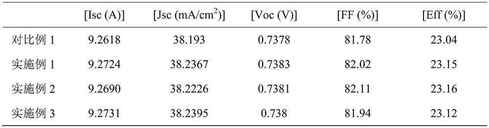
Embodiment 1
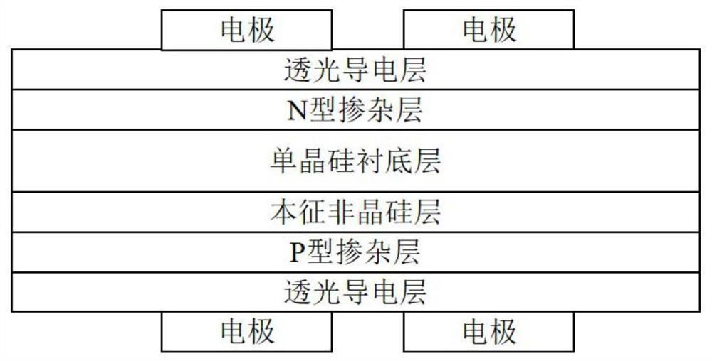
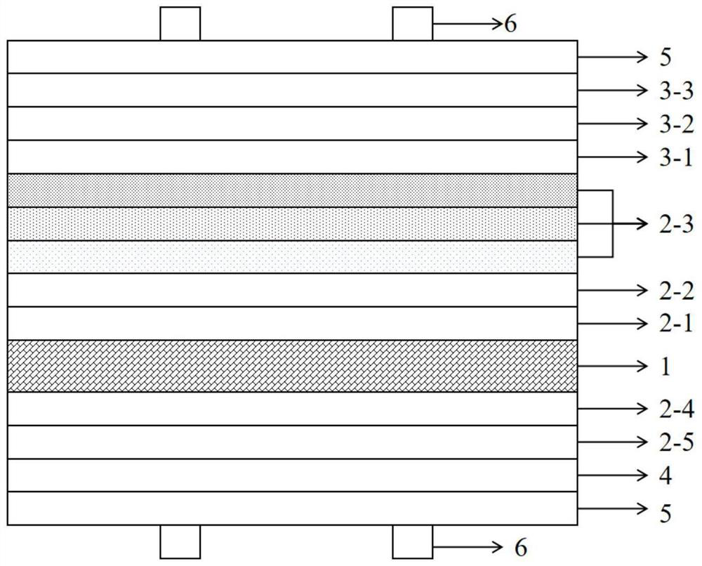
[0069] A heterojunction solar cell in this embodiment includes a base sheet, electrodes 6 arranged on the top surface and the bottom surface of the base sheet, and the base sheet includes:
[0070] Single crystal silicon substrate layer 1. The single crystal silicon substrate layer 1 in this embodiment is an N-type single crystal silicon substrate layer with a size of 156.75 mm and a thickness of 180 μm.
[0071] Two groups of intrinsic amorphous silicon layers, the two groups of intrinsic amorphous silicon layers include a first group of intrinsic amorphous silicon layers arranged on the top side of the single crystal silicon substrate layer 1 and a second group of intrinsic amorphous silicon layers arranged on the bottom side of the single crystal silicon substrate layer Two sets of intrinsic amorphous silicon layers.
[0072] The first group of intrinsic amorphous silicon layers includes the following three-layer structure arranged in sequence from the top side of the singl...
Embodiment 2
[0088]A high-efficiency silicon heterojunction solar cell of this embodiment is basically the same as that of Embodiment 1, except that:
[0089] The third intrinsic amorphous silicon layer 2-3, the third intrinsic amorphous silicon layer 2-3 is a stacked passivation layer deposited with silane and hydrogen gas, with a thickness of 6 nm.
[0090] In this embodiment, the third intrinsic amorphous silicon layer 2-3 includes the following three-layer structure arranged sequentially from the top side of the second intrinsic amorphous silicon layer 2-2 to the electrode direction:
[0091] The first passivation layer, the hydrogen and silane gas flow ratio of the first passivation layer is 3, the thickness is 1nm; the second passivation layer, the hydrogen and silane gas flow ratio of the second passivation layer is 5 , the thickness of which is 2nm; the third passivation layer, the flow ratio of hydrogen gas and silane gas of the third passivation layer is 10, and the thickness is ...
Embodiment 3
[0093] A heterojunction solar cell in this embodiment includes a base sheet, electrodes 6 arranged on the top surface and the bottom surface of the base sheet, and the base sheet includes:
[0094] Single crystal silicon substrate layer 1. The single crystal silicon substrate layer 1 in this embodiment is an N-type single crystal silicon substrate layer with a size of 156.75 mm and a thickness of 180 μm.
[0095] Two groups of intrinsic amorphous silicon layers, the two groups of intrinsic amorphous silicon layers include a first group of intrinsic amorphous silicon layers arranged on the top side of the single crystal silicon substrate layer 1 and a second group of intrinsic amorphous silicon layers arranged on the bottom side of the single crystal silicon substrate layer Two sets of intrinsic amorphous silicon layers.
[0096] The first group of intrinsic amorphous silicon layers includes the following three-layer structure arranged in sequence from the top side of the singl...
PUM
| Property | Measurement | Unit |
|---|---|---|
| Thickness | aaaaa | aaaaa |
| Thickness | aaaaa | aaaaa |
| Thickness | aaaaa | aaaaa |
Abstract
Description
Claims
Application Information