Silicon carbide fin-shaped gate MOSFET integrated with channel diode

A technology that integrates channels and diodes. It is used in climate sustainability, semiconductor devices, electrical components, etc., and can solve the problems of high conduction loss, large turn-on voltage, increased on-resistance and reverse leakage current, etc. The effect of improving withstand voltage and reliability, reducing on-resistance, and reducing reverse conduction voltage drop

Active Publication Date: 2021-07-16
UNIV OF ELECTRONICS SCI & TECH OF CHINA
View PDF21 Cites 7 Cited by
  • Summary
  • Abstract
  • Description
  • Claims
  • Application Information

AI Technical Summary

Problems solved by technology

Although using the body diode in SiC MOSFET as a freewheeling diode can save cost and area, the body diode of wide bandgap SiC material has a large turn-on voltage, which will lead to high conduction loss; at the same time, due to carrier recombination in SiC material The resulting bipolar degradation effect will cause adverse effects such as increased on-resistance and reverse leakage current.

Method used


Image

  • Silicon carbide fin-shaped gate MOSFET integrated with channel diode
  • Silicon carbide fin-shaped gate MOSFET integrated with channel diode

Examples


Embodiment 1

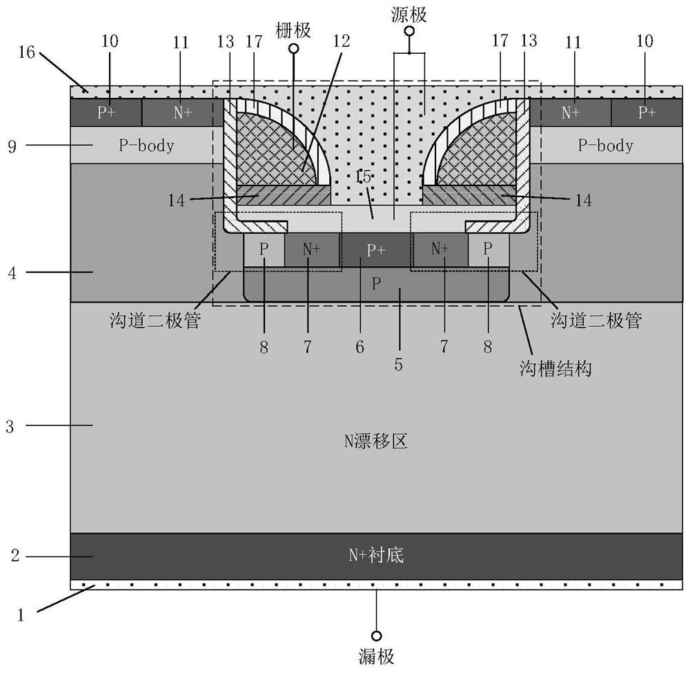
[0016] Such as figure 1 As shown, this example is a silicon carbide fin-gate MOSFET with integrated channel diode, which includes the first conductive material 1, N+ substrate layer 2, N drift region 3, epitaxial layer 4 and P -body region 9, the bottom of the first conductive material 1 is drawn out as a drain;

[0017] It is characterized in that it also includes a trench structure and a source region structure, the trench structure successively penetrates the P-body region 9 and the epitaxial layer 4 along the vertical direction, and then contacts the N drift region 3, and the source region structure is located in the trench The first P+ source contact region 10 and the first N+ source contact region 11 are arranged side by side on the upper surface of the P-body region 9 on both sides of the structure, wherein the first N+ source contact region 11 is in contact with the trench structure; the bottom of the trench structure is P The buried layer 5, the P buried layer 5 is i...

Embodiment 2

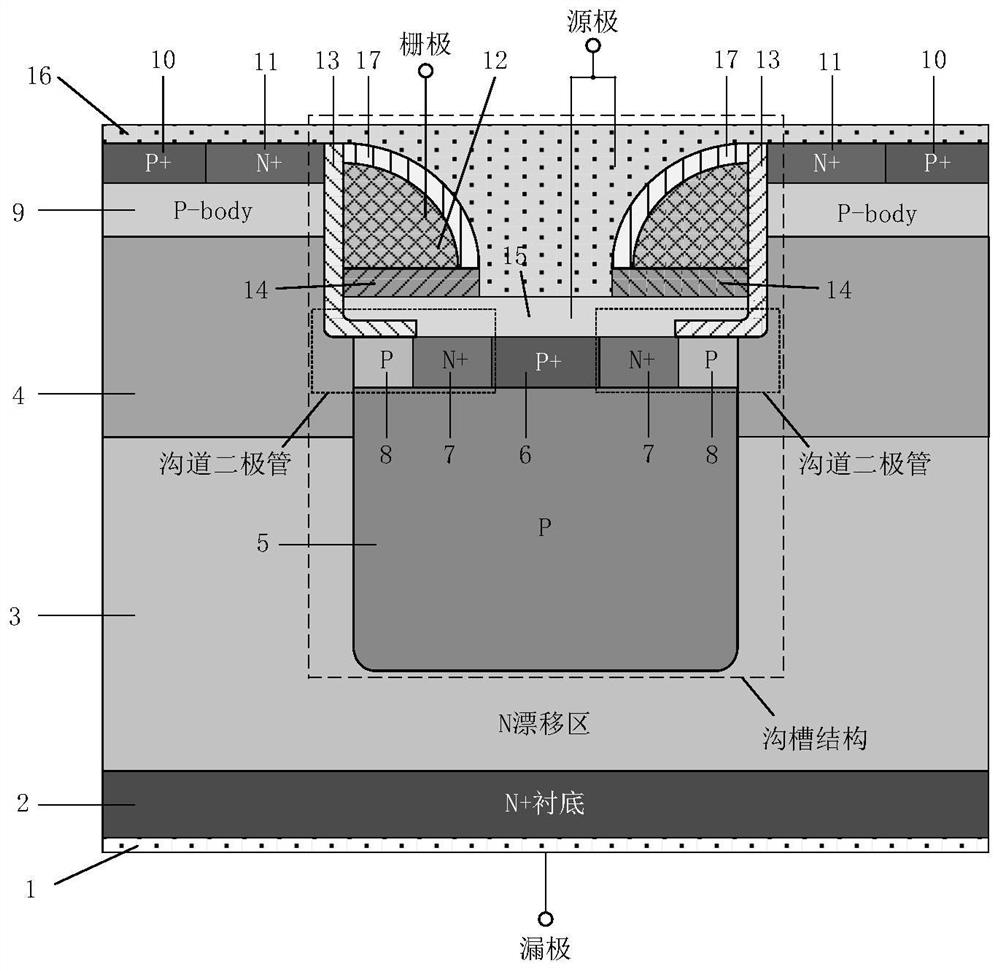
[0022] Such as figure 2 As shown, the difference between this example and Example 1 is that the P buried layer 5 extends downward into the N drift region 3, and the P buried layer 5 and the N drift region 3 form a semi-superjunction structure. In the off state, the semi-superjunction region forms a trapezoidal electric field distribution to improve the withstand voltage, and the higher doping concentration of the N drift region 3 in the forward conduction can reduce the on-resistance and improve the overall static characteristics of the device. Due to the existence of the P buried layer connected to the source potential at the bottom of the trench, the original gate-drain capacitance formed by the depletion of the bottom of the trench gate and the N drift region 3 will be converted into a gate-source capacitance, and the semi-superjunction structure will enhance this effect, making the device The gate-to-drain capacitance is further reduced.


PUM


Abstract

The invention belongs to the technical field of power semiconductors, and particularly relates to a silicon carbide fin-shaped gate MOSFET integrated with a channel diode. The silicon carbide fin-shaped gate MOSFET is mainly characterized in that the silicon carbide fin-shaped gate MOSFET is of a groove structure, the channel diode is integrated at the bottom part of a groove region, when the device is in a reverse follow current working mode, the channel diode is conducted to realize a follow current function, reverse conduction voltage drop is reduced, conduction of a body diode is effectively inhibited, and influence caused by bipolar degradation is eliminated; a fin-shaped gate structure is adopted, so that a P region below the groove is effectively grounded, a peak electric field of an oxide layer at the bottom part of the groove is lower than a critical breakdown value, and the reliability of the device in a blocking working mode is improved; and two symmetrical fin-shaped gates located in the groove and the third conductive material located at the bottom part of the groove below the fin-shaped gates form a composite separation gate structure, so that the gate-drain capacitance is reduced, the switching loss is reduced, and the device has more advantages in high-frequency application.

Description

technical field [0001] The invention belongs to the technical field of power semiconductors, and in particular relates to a silicon carbide fin gate MOSFET with integrated channel diodes. Background technique [0002] Compared with silicon (Si) materials, silicon carbide (SiC) has more superior physical properties due to its unique material properties, such as larger forbidden band width, higher saturation drift velocity and higher thermal conductivity. Static characteristics, high frequency characteristics and high temperature resistance characteristics are becoming more and more popular in the application of power devices. Compared with traditional SiC planar MOS devices, SiC trench gate MOS devices have lower on-resistance due to their larger channel density. However, SiC trench gate MOS devices have the problem that the peak electric field of the gate oxide layer is too large. In order to solve this problem, researchers have proposed a SiC fin gate MOSFET, which can ens...

Claims


Application Information

Patent Timeline
Patent Type & Authority Applications(China)
IPC IPC(8): H01L29/06H01L29/10H01L29/423H01L29/78H01L29/861H01L27/06
CPCH01L29/7827H01L29/785H01L29/1037H01L29/4236H01L27/0688H01L29/42356H01L29/063H01L29/0684H01L29/0623H01L29/8611Y02B70/10
Inventor 罗小蓉姜钦峰黄俊岳宋旭苏伟
Owner UNIV OF ELECTRONICS SCI & TECH OF CHINA
Why Eureka
Try Eureka